参数资料
| 型号: | EPCS16SI16N |
| 厂商: | Altera |
| 文件页数: | 20/40页 |
| 文件大小: | 0K |
| 描述: | IC CONFIG DEVICE 16MBIT 16-SOIC |
| 产品变化通告: | Product Discontinuation 01/31/2008 |
| 标准包装: | 49 |
| 系列: | EPCS |
| 可编程类型: | 系统内可编程 |
| 存储容量: | 16Mb |
| 电源电压: | 3 V ~ 3.6 V |
| 工作温度: | -40°C ~ 85°C |
| 封装/外壳: | 16-SOIC(0.295",7.50mm 宽) |
| 供应商设备封装: | 16-SOIC |
| 包装: | 管件 |
| 其它名称: | 544-1240-5 EPCS16SI16 |
第1页第2页第3页第4页第5页第6页第7页第8页第9页第10页第11页第12页第13页第14页第15页第16页第17页第18页第19页当前第20页第21页第22页第23页第24页第25页第26页第27页第28页第29页第30页第31页第32页第33页第34页第35页第36页第37页第38页第39页第40页
EPCS Device Memory Access
Page 27
Serial Configuration (EPCS) Devices Datasheet
January 2014
Altera Corporation
Figure 16 shows the instruction sequence of the erase bulk operation.
Erase Sector Operation
The erase sector operation code is b'1101 1000 and it lists the MSB first. This
operation allows you to erase a certain sector in the EPCS device by setting all the bits
inside the sector to 1 or 0xFF. This operation is useful if you want to access the unused
sectors as general purpose memory in your applications. You must execute the write
enable operation before the erase sector operation so that the write enable latch bit in
the status register is set to 1.
You can implement the erase sector operation by first driving the nCS signal low, then
you shift in the erase sector operation code, followed by the three address bytes of the
chosen sector on the ASDI pin. The three address bytes for the erase sector operation
can be any address inside the specified sector. For more information about the sector
address range, refer to Table 3 on page 7 through Table 7 on page 12. Drive the nCS
signal high after the eighth bit of the erase sector operation code has been latched in.
The device initiates the self-timed erase sector cycle immediately after the nCS signal is
driven high. For more information about the self-timed erase sector cycle time, refer to
You must account for this delay before accessing the memory contents. Alternatively,
you can check the write in progress bit in the status register by executing the read
status operation while the self-timed erase sector cycle is in progress. The write in
progress bit is set to 1 during the self-timed erase sector cycle and 0 when it is
complete. The write enable latch bit in the status register resets to 0 before the erase
cycle is complete.
Figure 17 shows the instruction sequence of the erase sector operation.
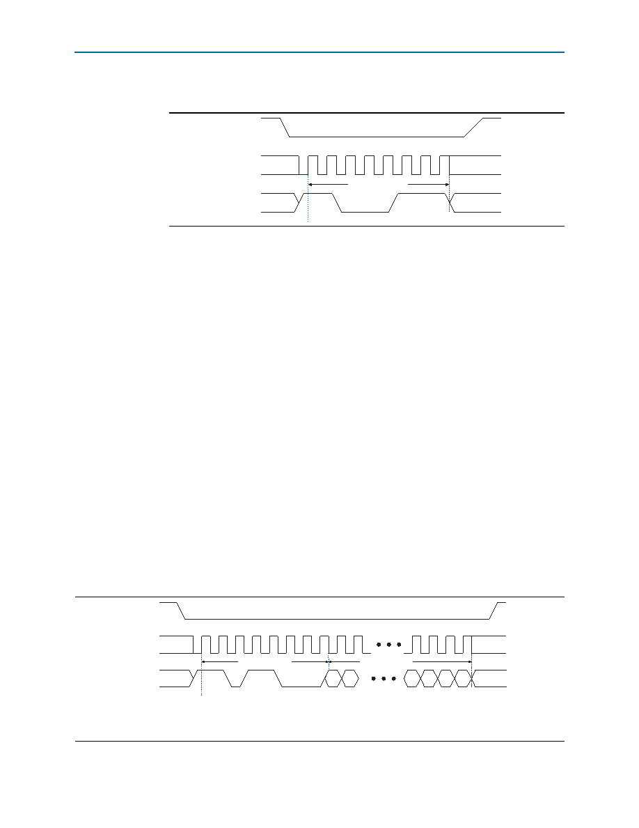
Figure 16. Erase Bulk Operation Timing Diagram
nCS
DCLK
ASDI
01234567
Operation Code
Figure 17. Erase Sector Operation Timing Diagram
Note to Figure 17:
(1) Address bit A[23] is a don't-care bit in the EPCS64 device. Address bits A[23..21] are don't-care bits in the EPCS16 device. Address bits
A[23..19]
are don't-care bits in the EPCS4 device. Address bits A[23..17] are don't-care bits in the EPCS1 device.
nCS
DCLK
ASDI
01234567
89
28
29
30
31
Operation Code
24-Bit Address (1)
23
22
3
2
1
0
MSB
相关PDF资料 |
PDF描述 |
|---|---|
| EPF10K10AQI208-3 | IC FLEX 10KA FPGA 10K 208-PQFP |
| EPF10K200EBC600-1 | IC FLEX 10KE FPGA 200K 600-BGA |
| EPF6024AQI208-3 | IC FLEX 6000 FPGA 24K 208-PQFP |
| EPF81500AQC240-2 | IC FLEX 8000A FPGA 16K 240-PQFP |
| EPM2210GF324C3 | IC MAX II CPLD 2210 LE 324-FBGA |
相关代理商/技术参数 |
参数描述 |
|---|---|
| EPCS16SI8N | 功能描述:FPGA-配置存储器 IC - Ser. Config Mem Flash 16Mb 40 MHz RoHS:否 制造商:Altera Corporation 存储类型:Flash 存储容量:1.6 Mbit 工作频率:10 MHz 电源电压-最大:5.25 V 电源电压-最小:3 V 电源电流:50 uA 最大工作温度:+ 85 C 最小工作温度:- 40 C 安装风格:SMD/SMT 封装 / 箱体:PLCC-20 |
| EPCS1N | 制造商:ALTERA 制造商全称:Altera Corporation 功能描述: |
| EPCS1SI8 | 功能描述:FPGA-配置存储器 IC - Ser. Config Mem Flash 1Mb 40 MHz RoHS:否 制造商:Altera Corporation 存储类型:Flash 存储容量:1.6 Mbit 工作频率:10 MHz 电源电压-最大:5.25 V 电源电压-最小:3 V 电源电流:50 uA 最大工作温度:+ 85 C 最小工作温度:- 40 C 安装风格:SMD/SMT 封装 / 箱体:PLCC-20 |
| EPCS1SI8N | 功能描述:FPGA-配置存储器 IC - Ser. Config Mem Flash 1Mb 40 MHz RoHS:否 制造商:Altera Corporation 存储类型:Flash 存储容量:1.6 Mbit 工作频率:10 MHz 电源电压-最大:5.25 V 电源电压-最小:3 V 电源电流:50 uA 最大工作温度:+ 85 C 最小工作温度:- 40 C 安装风格:SMD/SMT 封装 / 箱体:PLCC-20 |
| EPCS250 | 制造商:Electrolube 功能描述:COATING MASK PEELABLE 250 制造商:Electrolube 功能描述:COATING MASK, PEELABLE 250 |
发布紧急采购,3分钟左右您将得到回复。