- 您现在的位置:买卖IC网 > PDF目录295888 > EPM2210GF324A5N (ALTERA CORP) FLASH PLD, PBGA324 PDF资料下载
参数资料
| 型号: | EPM2210GF324A5N |
| 厂商: | ALTERA CORP |
| 元件分类: | PLD |
| 英文描述: | FLASH PLD, PBGA324 |
| 封装: | 19 X 19 MM, 1 MM PITCH, LEAD FREE, FBGA-324 |
| 文件页数: | 60/108页 |
| 文件大小: | 1342K |
| 代理商: | EPM2210GF324A5N |
第1页第2页第3页第4页第5页第6页第7页第8页第9页第10页第11页第12页第13页第14页第15页第16页第17页第18页第19页第20页第21页第22页第23页第24页第25页第26页第27页第28页第29页第30页第31页第32页第33页第34页第35页第36页第37页第38页第39页第40页第41页第42页第43页第44页第45页第46页第47页第48页第49页第50页第51页第52页第53页第54页第55页第56页第57页第58页第59页当前第60页第61页第62页第63页第64页第65页第66页第67页第68页第69页第70页第71页第72页第73页第74页第75页第76页第77页第78页第79页第80页第81页第82页第83页第84页第85页第86页第87页第88页第89页第90页第91页第92页第93页第94页第95页第96页第97页第98页第99页第100页第101页第102页第103页第104页第105页第106页第107页第108页
Altera Corporation
Core Version a.b.c variable
3–5
December 2007
MAX II Device Handbook, Volume 1
JTAG and In-System Programmability
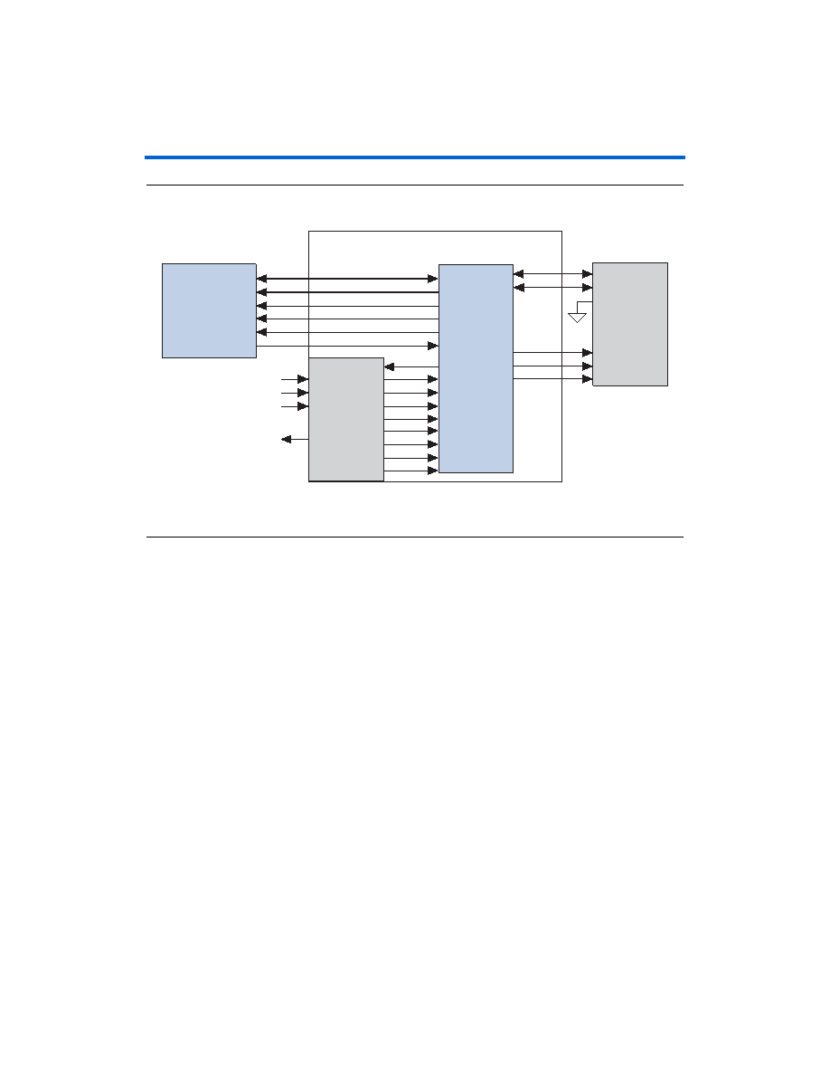
Figure 3–1. MAX II Parallel Flash Loader
Notes to Figure 3–1:
(1)
This block is implemented in LEs.
(2)
This function is supported in the Quartus II software.
In System
Programmability
MAX II devices can be programmed in-system via the industry standard
4-pin IEEE Std. 1149.1 (JTAG) interface. In-system programmability (ISP)
offers quick, efficient iterations during design development and
debugging cycles. The logic, circuitry, and interconnects in the MAX II
architecture are configured with flash-based SRAM configuration
elements. These SRAM elements require configuration data to be loaded
each time the device is powered. The process of loading the SRAM data
is called configuration. The on-chip configuration flash memory (CFM)
block stores the SRAM element’s configuration data. The CFM block
stores the design’s configuration pattern in a reprogrammable flash array.
During ISP, the MAX II JTAG and ISP circuitry programs the design
pattern into the CFM block’s non-volatile flash array.
The MAX II JTAG and ISP controller internally generate the high
programming voltages required to program the CFM cells, allowing
in-system programming with any of the recommended operating
external voltage supplies (that is, 3.3 V/2.5 V or 1.8 V for the MAX IIG
and MAX IIZ devices). ISP can be performed anytime after VCCINT and all
VCCIO banks have been fully powered and the device has completed the
configuration power-up time. By default, during in-system
Parallel
Flash Loader
Configuration
Logic
Flash
Memory Device
MAX II Device
DQ[7..0]
RY/BY
A[20..0]
OE
WE
CE
DQ[7..0]
RY/BY
A[20..0]
OE
WE
CE
TDI
TMS
TCK
TDI_U
TDO_U
TMS_U
TCK_U
SHIFT_U
CLKDR_U
UPDATE_U
RUNIDLE_U
USER1_U
TDO
Altera FPGA
CONF_DONE
nSTATUS
nCE
DCLK
DATA0
nCONFIG
(1), (2)
相关PDF资料 |
PDF描述 |
|---|---|
| EPM7064BFC100-3 | EE PLD, 3.5 ns, PBGA100 |
| EPM7064BFC100-5 | EE PLD, 3.5 ns, PBGA100 |
| EPM7064BFC100-7 | EE PLD, 3.5 ns, PBGA100 |
| EPM7064BTC100-3 | EE PLD, 3.5 ns, PQFP100 |
| EPM7064BTC100-5 | EE PLD, 3.5 ns, PQFP100 |
相关代理商/技术参数 |
参数描述 |
|---|---|
| EPM2210GF324C3 | 功能描述:CPLD - 复杂可编程逻辑器件 CPLD - MAX II 1700 Macro 272 IO RoHS:否 制造商:Lattice 系列: 存储类型:EEPROM 大电池数量:128 最大工作频率:333 MHz 延迟时间:2.7 ns 可编程输入/输出端数量:64 工作电源电压:3.3 V 最大工作温度:+ 90 C 最小工作温度:0 C 封装 / 箱体:TQFP-100 |
| EPM2210GF324C3N | 功能描述:CPLD - 复杂可编程逻辑器件 CPLD - MAX II 1700 Macro 272 IO RoHS:否 制造商:Lattice 系列: 存储类型:EEPROM 大电池数量:128 最大工作频率:333 MHz 延迟时间:2.7 ns 可编程输入/输出端数量:64 工作电源电压:3.3 V 最大工作温度:+ 90 C 最小工作温度:0 C 封装 / 箱体:TQFP-100 |
| EPM2210GF324C4 | 功能描述:CPLD - 复杂可编程逻辑器件 CPLD - MAX II 1700 Macro 272 IO RoHS:否 制造商:Lattice 系列: 存储类型:EEPROM 大电池数量:128 最大工作频率:333 MHz 延迟时间:2.7 ns 可编程输入/输出端数量:64 工作电源电压:3.3 V 最大工作温度:+ 90 C 最小工作温度:0 C 封装 / 箱体:TQFP-100 |
| EPM2210GF324C4N | 功能描述:CPLD - 复杂可编程逻辑器件 CPLD - MAX II 1700 Macro 272 IO RoHS:否 制造商:Lattice 系列: 存储类型:EEPROM 大电池数量:128 最大工作频率:333 MHz 延迟时间:2.7 ns 可编程输入/输出端数量:64 工作电源电压:3.3 V 最大工作温度:+ 90 C 最小工作温度:0 C 封装 / 箱体:TQFP-100 |
| EPM2210GF324C5 | 功能描述:CPLD - 复杂可编程逻辑器件 CPLD - MAX II 1700 Macro 272 IO RoHS:否 制造商:Lattice 系列: 存储类型:EEPROM 大电池数量:128 最大工作频率:333 MHz 延迟时间:2.7 ns 可编程输入/输出端数量:64 工作电源电压:3.3 V 最大工作温度:+ 90 C 最小工作温度:0 C 封装 / 箱体:TQFP-100 |
发布紧急采购,3分钟左右您将得到回复。