- 您现在的位置:买卖IC网 > PDF目录16559 > EV-ADF4157SD1Z (Analog Devices Inc)BOARD EVAL FOR ADF4157 PDF资料下载
参数资料
| 型号: | EV-ADF4157SD1Z |
| 厂商: | Analog Devices Inc |
| 文件页数: | 21/24页 |
| 文件大小: | 0K |
| 描述: | BOARD EVAL FOR ADF4157 |
| 标准包装: | 1 |
| 主要目的: | 计时,频率合成器 |
| 嵌入式: | 否 |
| 已用 IC / 零件: | ADF4157 |
| 主要属性: | 单路分数-N PLL |
| 次要属性: | 6GHz |
| 已供物品: | 板 |
ADF4157
Data Sheet
Rev. D | Page 6 of 24
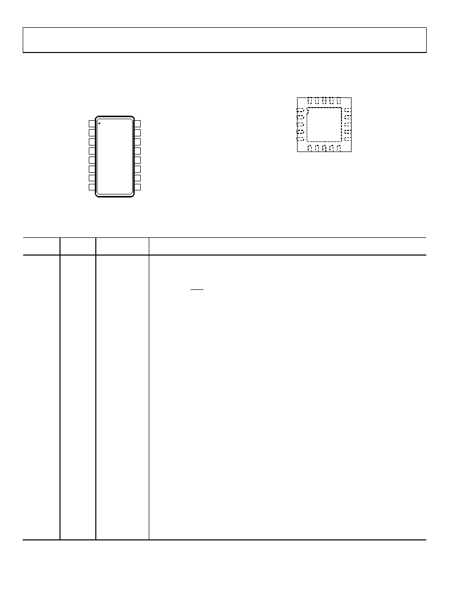
PIN CONFIGURATIONS AND FUNCTION DESCRIPTIONS
1
2
3
4
5
6
7
8
16
15
14
13
12
11
10
9
CP
CPGND
AGND
AVDD
RFINA
RFINB
RSET
DVDD
MUXOUT
LE
CE
REFIN
DGND
CLK
DATA
VP
ADF4157
TOP VIEW
(Not to Scale)
05
87
4-
00
3
Figure 3. TSSOP Pin Configuration
0
587
4-
00
4
NOTES
1. IT IS RECOMMENDED THAT THE EXPOSED PAD
BE THERMALLY CONNECTED TO A COPPER
PLANE FOR ENHANCED THERMAL PERFORMANCE.
THIS PAD SHOULD BE CONNECTED TO AGND.
14
13
12
1
3
4
LE
15 MUXOUT
DATA
CLK
11 CE
CPGND
AGND
2
AGND
RFINB
5
RFINA
7
A
V
D
6
A
V
D
8
R
E
F
IN
9
D
G
N
D
1
0
D
G
N
D
1
9
R
S
E
T
2
0
C
P
1
8
V
P
1
7
D
V
D
1
6
D
V
D
ADF4157
TOP VIEW
(Not to Scale)
Figure 4. LFCSP Pin Configuration
Table 5. Pin Function Descriptions
TSSOP
Pin No.
LFCSP
Pin No.
Mnemonic
Description
1
19
RSET
Connecting a resistor between this pin and ground sets the maximum charge pump output
current.
The relationship between ICP and RSET is
SET
CPMAX
R
I
5
.
25
where:
RSET = 5.1 kΩ.
ICPMAX = 5 mA.
2
20
CP
Charge Pump Output. When enabled, this pin provides ±ICP to the external loop filter, which, in
turn, drives the external VCO.
3
1
CPGND
Charge Pump Ground. This is the ground return path for the charge pump.
4
2, 3
AGND
Analog Ground. This is the ground return path of the prescaler.
5
4
RFINB
Complementary Input to the RF Prescaler. This point should be decoupled to the ground plane
with a small bypass capacitor, typically 100 pF.
6
5
RFINA
Input to the RF Prescaler. This small-signal input is normally ac-coupled from the VCO.
7
6, 7
AVDD
Positive Power Supply for the RF Section. Decoupling capacitors to the digital ground plane
should be placed as close as possible to this pin. AVDD has a value of 3 V ± 10%. AVDD must have
the same voltage as DVDD.
8
REFIN
Reference Input. This is a CMOS input with a nominal threshold of VDD/2 and an equivalent
input resistance of 100 kΩ. This input can be driven from a TTL or CMOS crystal oscillator, or it
can be ac-coupled.
9
9, 10
DGND
Digital Ground.
10
11
CE
Chip Enable. A logic low on this pin powers down the device and puts the charge pump output
into three-state mode.
11
12
CLK
Serial Clock Input. This serial clock is used to clock in the serial data to the registers. The data is
latched into the input shift register on the CLK rising edge. This input is a high impedance
CMOS input.
12
13
DATA
Serial Data Input. The serial data is loaded MSB first with the three LSBs being the control bits.
This input is a high impedance CMOS input.
13
14
LE
Load Enable, CMOS Input. When LE is high, the data stored in the input shift register is loaded
into one of the five latches, with the latch selected using the control bits.
14
15
MUXOUT
This multiplexer output allows the lock detect, the scaled RF, or the scaled reference frequency
to be accessed externally.
相关PDF资料 |
PDF描述 |
|---|---|
| V48C24E150BG2 | CONVERTER MOD DC/DC 24V 150W |
| MCP100T-300I/TT | IC SUPERVISOR ACTIVE LOW SOT23-3 |
| GMM10DRTS | CONN EDGECARD 20POS DIP .156 SLD |
| A2MXS-2636M | ADM26S/AE26M/X |
| GSM10DREI | CONN EDGECARD 20POS .156 EYELET |
相关代理商/技术参数 |
参数描述 |
|---|---|
| EV-ADF4159EB1Z | 制造商:Analog Devices 功能描述:EVALUATION BOARD - Boxed Product (Development Kits) 制造商:Analog Devices 功能描述:EVAL BOARD FOR ADF4159 |
| EV-ADF4159EB2Z | 制造商:Analog Devices 功能描述:13GHZFRAC-NPLL+ADF55XXVCO+3VADM - Boxed Product (Development Kits) |
| EV-ADF4159EB3Z | 制造商:Analog Devices 功能描述:EVALUATIONBOARD - Boxed Product (Development Kits) 制造商:Analog Devices 功能描述:EVAL BOARD FOR ADF4159 制造商:Analog Devices 功能描述:Clock & Timer Development Tools ADF4159 EVAL BRD |
| EV-ADF4360-0EB1Z | 功能描述:BOARD EVAL FOR ADF4360-0 RoHS:是 类别:编程器,开发系统 >> 评估演示板和套件 系列:- 标准包装:1 系列:- 主要目的:电信,线路接口单元(LIU) 嵌入式:- 已用 IC / 零件:IDT82V2081 主要属性:T1/J1/E1 LIU 次要属性:- 已供物品:板,电源,线缆,CD 其它名称:82EBV2081 |
| EV-ADF4360-1EB1Z | 功能描述:BOARD EVAL FOR ADF4360-1 RoHS:是 类别:编程器,开发系统 >> 评估演示板和套件 系列:- 标准包装:1 系列:- 主要目的:电信,线路接口单元(LIU) 嵌入式:- 已用 IC / 零件:IDT82V2081 主要属性:T1/J1/E1 LIU 次要属性:- 已供物品:板,电源,线缆,CD 其它名称:82EBV2081 |
发布紧急采购,3分钟左右您将得到回复。