- 您现在的位置:买卖IC网 > PDF目录16562 > EV-ADF4360-7EB1Z (Analog Devices Inc)BOARD EVAL FOR ADF4360-7 PDF资料下载
参数资料
| 型号: | EV-ADF4360-7EB1Z |
| 厂商: | Analog Devices Inc |
| 文件页数: | 15/28页 |
| 文件大小: | 0K |
| 描述: | BOARD EVAL FOR ADF4360-7 |
| 标准包装: | 1 |
| 主要目的: | 计时,频率合成器 |
| 嵌入式: | 否 |
| 已用 IC / 零件: | ADF4360-7 |
| 主要属性: | 带 VCO 的单路整数-N PLL |
| 次要属性: | 900MHz,200kHz PFD |
| 已供物品: | 板,缆线,CD |
第1页第2页第3页第4页第5页第6页第7页第8页第9页第10页第11页第12页第13页第14页当前第15页第16页第17页第18页第19页第20页第21页第22页第23页第24页第25页第26页第27页第28页
ADF4360-7
Data Sheet
Rev. D | Page 22 of 28
CHOOSING THE CORRECT INDUCTANCE VALUE
The ADF4360-7 can be used at many different frequencies
simply by choosing the external inductors to give the correct
output frequency. Figure 24 shows a graph of both minimum
and maximum frequency vs. the external inductor value. The
correct inductor should cover the maximum and minimum
frequencies desired. The inductors used are the 0402 CS type
from Coilcraft. To reduce mutual coupling, the inductors
should be placed at right angles to one another.
As shown in Figure 24, the lowest commercially available value
of inductance, 1.0 nH, sets the center frequency at approximate-
ly 1300 MHz. For inductances less than 2.4 nH, a PCB trace
should be used, a direct short. The lowest center
frequency of oscillation possible is approximately 350 MHz,
which is achieved using 30 nH inductors. This relationship
can be expressed by
(
)
EXT
O
L
F
+
=
nH
0.9
pF
6.2
2π
1
where FO is the center frequency, and LEXT is the external in-
ductance.
300
500
400
1200
1300
1400
1000
1100
800
900
600
700
1500
0
5
10
15
20
30
25
EXT INDUCTANCE (nH)
FREQUENCY
(MHz)
04441-028
Figure 24. Output Center Frequency vs. External Inductor Value
The approximate value of capacitance at the midpoint of the
center band of the VCO is 6.2 pF, and the approximate value of
internal inductance due to the bond wires is 0.9 nH. The VCO
sensitivity is a measure of the frequency change vs. the tuning
voltage. It is a very important parameter for the low-pass filter.
Figure 25 shows a graph of the tuning sensitivity (in MHz/V)
vs. the inductance (nH). It can be seen that as the inductance
increases, the sensitivity decreases. This relationship can be
derived from the previous equation, i.e., because the inductance
has increased, the change in capacitance from the varactor has
less of an effect on the frequency.
0
5
30
25
20
15
10
35
0
10
20
40
30
EXT INDUCTANCE (nH)
SENSITIVITY
(MHz/V)
04441-029
Figure 25. Tuning Sensitivity (in MHz/V) vs. Inductance (nH)
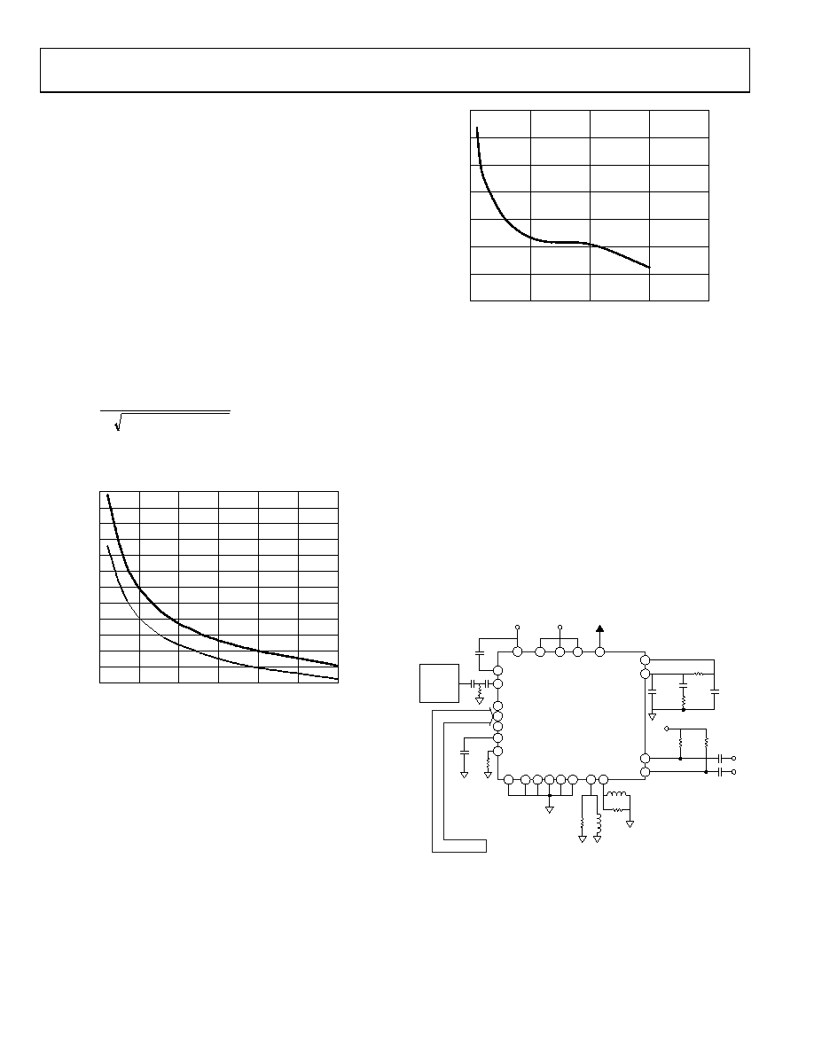
FIXED FREQUENCY LO
Figure 26 shows the ADF4360-7 used as a fixed frequency LO at
500 MHz. The low-pass filter was designed using ADIsimPLL
for a channel spacing of 8 MHz and an open-loop bandwidth of
30 kHz. The maximum PFD frequency of the ADF4360-7 is
8 MHz. Because using a larger PFD frequency allows the use of
a smaller N, the in-band phase noise is reduced to as low as
possible, 109 dBc/Hz. The typical rms phase noise (100 Hz to
100 kHz) of the LO in this configuration is 0.3°. The reference
frequency is from a 16 MHz TCXO from Fox; thus, an R value of
2 is programmed. Taking into account the high PFD frequency
and its effect on the band select logic, the band select clock
divider is enabled. In this case, a value of 8 is chosen. A very sim-
ple pull-up resistor and dc blocking capacitor complete the RF
output stage.
SPI
COMPATIBLE
SERIAL
BUS
ADF4360-7
VVCO
FOX
801BE-160
16MHz
VVCO
CPGND
AGND DGND L1 L2 RF
OUTB
RFOUTA
CP
1nF
2.7nF
13nH
470
13nH
470
820pF
27nF
51
51
51
100pF
1nF
10
F
4.7k
510
910
RSET
CC
LE
DATA
CLK
REFIN
CN
VTUNE
DVDD AVDD CE MUXOUT
5
4
24
7
20
23
2
21
6
14
16
17
18
19
13
1
3
8
9
10
11 22
15
12
VVDD
LOCK
DETECT
04441-030
Figure 26. Fixed Frequency LO
相关PDF资料 |
PDF描述 |
|---|---|
| RCC15DRTF | CONN EDGECARD 30POS DIP .100 SLD |
| RSA06DRMH-S288 | CONN EDGECARD 12POS .125 EXTEND |
| SLF7055T-1R5N4R0-3PF | INDUCTOR POWER 1.5UH 4.0A SMD |
| RCC18DRAN | CONN EDGECARD 36POS R/A .100 SLD |
| RMA06DRMH-S288 | CONN EDGECARD 12POS .125 EXTEND |
相关代理商/技术参数 |
参数描述 |
|---|---|
| EV-ADF4360-8EB1Z | 功能描述:BOARD EVALUATION FOR ADF4360-8 RoHS:是 类别:编程器,开发系统 >> 评估演示板和套件 系列:- 标准包装:1 系列:- 主要目的:电信,线路接口单元(LIU) 嵌入式:- 已用 IC / 零件:IDT82V2081 主要属性:T1/J1/E1 LIU 次要属性:- 已供物品:板,电源,线缆,CD 其它名称:82EBV2081 |
| EV-ADF4360-9EB1Z | 功能描述:BOARD EVAL FOR ADF4360-9 RoHS:是 类别:编程器,开发系统 >> 评估演示板和套件 系列:- 标准包装:1 系列:- 主要目的:电信,线路接口单元(LIU) 嵌入式:- 已用 IC / 零件:IDT82V2081 主要属性:T1/J1/E1 LIU 次要属性:- 已供物品:板,电源,线缆,CD 其它名称:82EBV2081 |
| EV-ADF4602EB3ZTST | 制造商:Analog Devices 功能描述:BASEBAND ADAPTER BOARD - Boxed Product (Development Kits) |
| EV-ADUCRF101MK1Z | 制造商:Analog Devices 功能描述:EVALUATION BOARD WITH USB - Boxed Product (Development Kits) |
| EV-ADUCRF101MK1ZU1 | 制造商:Analog Devices 功能描述:DEVELOPMENT TOOL - Boxed Product (Development Kits) |
发布紧急采购,3分钟左右您将得到回复。