- 您现在的位置:买卖IC网 > PDF目录16562 > EV-ADF4360-7EB1Z (Analog Devices Inc)BOARD EVAL FOR ADF4360-7 PDF资料下载
参数资料
| 型号: | EV-ADF4360-7EB1Z |
| 厂商: | Analog Devices Inc |
| 文件页数: | 16/28页 |
| 文件大小: | 0K |
| 描述: | BOARD EVAL FOR ADF4360-7 |
| 标准包装: | 1 |
| 主要目的: | 计时,频率合成器 |
| 嵌入式: | 否 |
| 已用 IC / 零件: | ADF4360-7 |
| 主要属性: | 带 VCO 的单路整数-N PLL |
| 次要属性: | 900MHz,200kHz PFD |
| 已供物品: | 板,缆线,CD |
第1页第2页第3页第4页第5页第6页第7页第8页第9页第10页第11页第12页第13页第14页第15页当前第16页第17页第18页第19页第20页第21页第22页第23页第24页第25页第26页第27页第28页
Data Sheet
ADF4360-7
Rev. D | Page 23 of 28
INTERFACING
The ADF4360 family has a simple SPI-compatible serial inter-
face for writing to the device. CLK, DATA, and LE control the
data transfer. When LE goes high, the 24 bits that have been
clocked into the appropriate register on each rising edge of CLK
are transferred to the appropriate latch. See Figure 2 for the
timing diagram and Table 5 for the latch truth table.
The maximum allowable serial clock rate is 20 MHz. This
means that the maximum update rate possible is 833 kHz or
one update every 1.2 s. This is certainly more than adequate
for systems that have typical lock times in hundreds of micro-
seconds.
ADuC812 Interface
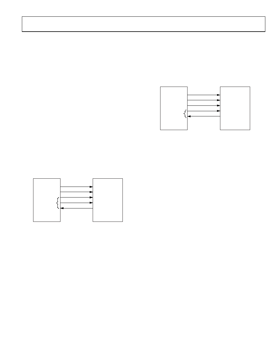
Figure 27 shows the interface between the ADF4360 family and
the ADuC812 MicroConverter. Because the ADuC812 is based
on an 8051 core, this interface can be used with any 8051-based
microcontroller. The MicroConverter is set up for SPI master
mode with CPHA = 0. To initiate the operation, the I/O port
driving LE is brought low. Each latch of the ADF4360 family
needs a 24-bit word, which is accomplished by writing three
8-bit bytes from the MicroConverter to the device. After the
third byte has been written, the LE input should be brought
high to complete the transfer.
04441-031
ADuC812
ADF4360-x
SCLK
SDATA
LE
CE
MUXOUT
(LOCK DETECT)
SCLOCK
MOSI
I/O PORTS
Figure 27. ADuC812 to ADF4360-x Interface
I/O port lines on the ADuC812 are also used to control pow-
erdown (CE input) and detect lock (MUXOUT configured as
lock detect and polled by the port input). When operating in
the described mode, the maximum SCLOCK rate of the
ADuC812 is 4 MHz. This means that the maximum rate at
which the output frequency can be changed is 166 kHz.
ADSP-2181 Interface
Figure 28 shows the interface between the ADF4360 family and
the ADSP-21xx digital signal processor. The ADF4360 family
needs a 24-bit serial word for each latch write. The easiest way
to accomplish this using the ADSP-21xx family is to use the
autobuffered transmit mode of operation with alternate fram-
ing. This provides a means for transmitting an entire block of
serial data before an interrupt is generated.
04441-032
ADSP-21xx
ADF4360-x
SCLK
SDATA
LE
CE
MUXOUT
(LOCK DETECT)
SCLOCK
MOSI
TFS
I/O PORTS
Figure 28. ADSP-21xx to ADF4360-x Interface
Set up the word length for 8 bits and use three memory loca-
tions for each 24-bit word. To program each 24-bit latch, store
the 8-bit bytes, enable the autobuffered mode, and write to the
transmit register of the DSP. This last operation initiates the
autobuffer transfer.
PCB DESIGN GUIDELINES FOR CHIP SCALE PACKAGE
The leads on the chip scale package (CP-24) are rectangular.
The printed circuit board pad for these should be 0.1 mm long-
er than the package lead length and 0.05 mm wider than the
package lead width. The lead should be centered on the pad to
ensure that the solder joint size is maximized.
The bottom of the chip scale package has a central thermal pad.
The thermal pad on the printed circuit board should be at least
as large as this exposed pad. On the printed circuit board, there
should be a clearance of at least 0.25 mm between the thermal
pad and the inner edges of the pad pattern to ensure that short-
ing is avoided.
Thermal vias may be used on the printed circuit board thermal
pad to improve thermal performance of the package. If vias
are used, they should be incorporated into the thermal pad at a
1.2 mm pitch grid. The via diameter should be between 0.3 mm
and 0.33 mm, and the via barrel should be plated with 1 ounce
of copper to plug the via.
The user should connect the printed circuit thermal pad to
AGND. This is internally connected to AGND.
相关PDF资料 |
PDF描述 |
|---|---|
| RCC15DRTF | CONN EDGECARD 30POS DIP .100 SLD |
| RSA06DRMH-S288 | CONN EDGECARD 12POS .125 EXTEND |
| SLF7055T-1R5N4R0-3PF | INDUCTOR POWER 1.5UH 4.0A SMD |
| RCC18DRAN | CONN EDGECARD 36POS R/A .100 SLD |
| RMA06DRMH-S288 | CONN EDGECARD 12POS .125 EXTEND |
相关代理商/技术参数 |
参数描述 |
|---|---|
| EV-ADF4360-8EB1Z | 功能描述:BOARD EVALUATION FOR ADF4360-8 RoHS:是 类别:编程器,开发系统 >> 评估演示板和套件 系列:- 标准包装:1 系列:- 主要目的:电信,线路接口单元(LIU) 嵌入式:- 已用 IC / 零件:IDT82V2081 主要属性:T1/J1/E1 LIU 次要属性:- 已供物品:板,电源,线缆,CD 其它名称:82EBV2081 |
| EV-ADF4360-9EB1Z | 功能描述:BOARD EVAL FOR ADF4360-9 RoHS:是 类别:编程器,开发系统 >> 评估演示板和套件 系列:- 标准包装:1 系列:- 主要目的:电信,线路接口单元(LIU) 嵌入式:- 已用 IC / 零件:IDT82V2081 主要属性:T1/J1/E1 LIU 次要属性:- 已供物品:板,电源,线缆,CD 其它名称:82EBV2081 |
| EV-ADF4602EB3ZTST | 制造商:Analog Devices 功能描述:BASEBAND ADAPTER BOARD - Boxed Product (Development Kits) |
| EV-ADUCRF101MK1Z | 制造商:Analog Devices 功能描述:EVALUATION BOARD WITH USB - Boxed Product (Development Kits) |
| EV-ADUCRF101MK1ZU1 | 制造商:Analog Devices 功能描述:DEVELOPMENT TOOL - Boxed Product (Development Kits) |
发布紧急采购,3分钟左右您将得到回复。