- 您现在的位置:买卖IC网 > PDF目录16561 > EV-ADF4360-9EB1Z (Analog Devices Inc)BOARD EVAL FOR ADF4360-9 PDF资料下载
参数资料
| 型号: | EV-ADF4360-9EB1Z |
| 厂商: | Analog Devices Inc |
| 文件页数: | 16/24页 |
| 文件大小: | 0K |
| 描述: | BOARD EVAL FOR ADF4360-9 |
| 标准包装: | 1 |
| 主要目的: | 计时,频率合成器 |
| 嵌入式: | 否 |
| 已用 IC / 零件: | ADF4360-9 |
| 主要属性: | 带 VCO 的单路整数-N PLL |
| 次要属性: | 360MHz,1.6MHz PFD |
| 已供物品: | 板,缆线,CD |
Data Sheet
ADF4360-9
Rev. C | Page 23 of 24
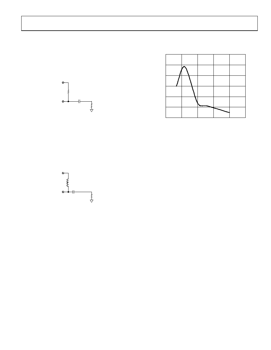
OUTPUT MATCHING
There are a number of ways to match the VCO output of the
ADF4360-9 for optimum operation; the most basic is to use a
51 resistor to VVCO. A dc bypass capacitor of 100 pF is connected
in series, as shown in Figure 33. Because the resistor is not
frequency dependent, this provides a good broadband match.
The output power in the circuit in Figure 33 typically gives
9 dBm output power into a 50 load.
100pF
07139-
030
RFOUT
VVCO
50
51
Figure 33. Simple Output Stage
A better solution is to use a shunt inductor (acting as an RF
choke) to VVCO. This gives a better match and, therefore, more
output power.
Experiments have shown that the circuit shown in Figure 34
provides an excellent match to 50 over the operating range of
the ADF4360-9. This gives approximately 0 dBm output power
across the specific frequency range of the ADF4360-9 using the
recommended shunt inductor, followed by a 100 pF dc-blocking
capacitor.
L
100pF
07139-
031
RFOUT
VVCO
50
Figure 34. Optimum Output Stage
The recommended value of this inductor changes with the VCO
center frequency. Figure 35 shows a graph of the optimum
inductor value vs. center frequency.
CENTER FREQUENCY (MHz)
INDUC
T
ANCE
(
n
H)
300
250
150
200
100
0
50
0
100
200
300
500
400
07139-
032
Figure 35. Optimum Shunt Inductor vs. Center Frequency
Both complementary architectures can be examined using the
EV-ADF4360-9EB1Z evaluation board. If the user does not
need the differential outputs available on the ADF4360-9, the
user should either terminate the unused output with the same
circuitry as much as possible or combine both outputs using a
balun. Alternatively, instead of the LC balun, both outputs can
be combined using a 180° rat-race coupler.
If the user is only using DIVOUT and does not use the RF
outputs, it is still necessary to terminate both RF output pins
with a shunt inductor/resistor to VVCO and also a dc bypass
capacitor and a 50 load. The circuit in Figure 33 is probably
the simplest and most cost-effective solution. It is important
that the load on each pin be balanced because an unbalanced
load is likely to cause stability problems. Terminations should
be identical as much as possible.
相关PDF资料 |
PDF描述 |
|---|---|
| A6MMS-2636G | IDC CABLE - ADM26S/AE26G/ADM26S |
| M2MXH-1440K | IDC CABLE - MDM14H/MC14F/X |
| H3DWH-2618M | IDC CABLE - HKR26H/AE26M/HPL26H |
| EV-ADF4360-0EB1Z | BOARD EVAL FOR ADF4360-0 |
| H3DKH-2618M | IDC CABLE - HKR26H/AE26M/HPK26H |
相关代理商/技术参数 |
参数描述 |
|---|---|
| EV-ADF4602EB3ZTST | 制造商:Analog Devices 功能描述:BASEBAND ADAPTER BOARD - Boxed Product (Development Kits) |
| EV-ADUCRF101MK1Z | 制造商:Analog Devices 功能描述:EVALUATION BOARD WITH USB - Boxed Product (Development Kits) |
| EV-ADUCRF101MK1ZU1 | 制造商:Analog Devices 功能描述:DEVELOPMENT TOOL - Boxed Product (Development Kits) |
| EV-ADUCRF101MK3ZU1 | 制造商:Analog Devices 功能描述:EVALUATION BOARD - Boxed Product (Development Kits) |
| EVA-EC-DASHBOARD-001 | 制造商:Renesas Electronics Corporation 功能描述:78K0 REF BD 78K0/DF2 MCU 制造商:Renesas Electronics Corporation 功能描述:EVA-EC-DASHBOARD-001 - Boxed Product (Development Kits) 制造商:Renesas Electronics Corporation 功能描述:EVALUATION BOARD |
发布紧急采购,3分钟左右您将得到回复。