- 您现在的位置:买卖IC网 > PDF目录16561 > EV-ADF4360-9EB1Z (Analog Devices Inc)BOARD EVAL FOR ADF4360-9 PDF资料下载
参数资料
| 型号: | EV-ADF4360-9EB1Z |
| 厂商: | Analog Devices Inc |
| 文件页数: | 2/24页 |
| 文件大小: | 0K |
| 描述: | BOARD EVAL FOR ADF4360-9 |
| 标准包装: | 1 |
| 主要目的: | 计时,频率合成器 |
| 嵌入式: | 否 |
| 已用 IC / 零件: | ADF4360-9 |
| 主要属性: | 带 VCO 的单路整数-N PLL |
| 次要属性: | 360MHz,1.6MHz PFD |
| 已供物品: | 板,缆线,CD |
ADF4360-9
Data Sheet
Rev. C | Page 10 of 24
CIRCUIT DESCRIPTION
REFERENCE INPUT SECTION
The reference input stage is shown in Figure 16. SW1 and SW2
are normally closed switches, and SW3 is normally open. When
power-down is initiated, SW3 is closed, and SW1 and SW2 are
opened. This ensures that there is no loading of the REFIN pin at
power-down.
07139-
016
BUFFER
TO R COUNTER
REFIN
100k
NC
SW2
SW3
NO
NC
SW1
POWER-DOWN
CONTROL
Figure 16. Reference Input Stage
N COUNTER
The CMOS N counter allows a wide division ratio in the PLL
feedback counter. The counters are specified to work when the
VCO output is 400 MHz or less. To avoid confusion, this is
referred to as the B counter. It makes it possible to generate
output frequencies that are spaced only by the reference
frequency divided by R. The VCO frequency equation is
fVCO = B × fREFIN/R
where:
fVCO is the output frequency of the VCO.
B is the preset divide ratio of the binary 13-bit counter (3 to 8191).
fREFIN is the external reference frequency oscillator.
R COUNTER
The 14-bit R counter allows the input reference frequency
to be divided down to produce the reference clock to the phase
frequency detector (PFD). Division ratios from 1 to 16,383 are
allowed.
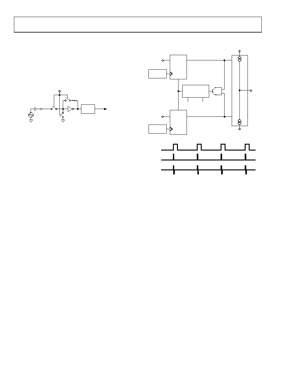
PFD AND CHARGE PUMP
The PFD takes inputs from the R counter and N counter (N = B)
and produces an output proportional to the phase and frequency
difference between them. Figure 17 is a simplified schematic.
The PFD includes a programmable delay element that controls
the width of the antibacklash pulse. This pulse ensures that
there is no dead zone in the PFD transfer function and
minimizes phase noise and reference spurs. Two bits in the R
counter latch, ABP2 and ABP1, control the width of the pulse
07139-
017
PROGRAMMABLE
DELAY
U3
CLR2
Q2
D2
U2
CLR1
Q1
D1
CHARGE
PUMP
DOWN
UP
HI
U1
ABP1
ABP2
R DIVIDER
N DIVIDER
CP OUTPUT
R DIVIDER
N DIVIDER
CP
CPGND
VP
Figure 17. PFD Simplified Schematic and Timing (In Lock)
LOCK DETECT
The LD pin outputs a lock detect signal. Digital lock detect is
active high. When lock detect precision (LDP) in the R counter
latch is set to 0, digital lock detect is set high when the phase error
on three consecutive phase detector cycles is <15 ns.
When LDP is set to 1, five consecutive cycles of <15 ns phase
error are required to set the lock detect. It stays set high until a
phase error of >25 ns is detected on any subsequent PD cycle.
INPUT SHIFT REGISTER
The digital section of the ADF4360 family includes a 24-bit
input shift register, a 14-bit R counter, and an 18-bit N counter,
comprising a 5-bit A counter and a 13-bit B counter. Data is
clocked into the 24-bit shift register on each rising edge of CLK.
The data is clocked in MSB first. Data is transferred from the
shift register to one of four latches on the rising edge of LE. The
destination latch is determined by the state of the two control
bits (C2, C1) in the shift register. The two LSBs, DB1 and DB0,
are shown in Figure 2.
相关PDF资料 |
PDF描述 |
|---|---|
| A6MMS-2636G | IDC CABLE - ADM26S/AE26G/ADM26S |
| M2MXH-1440K | IDC CABLE - MDM14H/MC14F/X |
| H3DWH-2618M | IDC CABLE - HKR26H/AE26M/HPL26H |
| EV-ADF4360-0EB1Z | BOARD EVAL FOR ADF4360-0 |
| H3DKH-2618M | IDC CABLE - HKR26H/AE26M/HPK26H |
相关代理商/技术参数 |
参数描述 |
|---|---|
| EV-ADF4602EB3ZTST | 制造商:Analog Devices 功能描述:BASEBAND ADAPTER BOARD - Boxed Product (Development Kits) |
| EV-ADUCRF101MK1Z | 制造商:Analog Devices 功能描述:EVALUATION BOARD WITH USB - Boxed Product (Development Kits) |
| EV-ADUCRF101MK1ZU1 | 制造商:Analog Devices 功能描述:DEVELOPMENT TOOL - Boxed Product (Development Kits) |
| EV-ADUCRF101MK3ZU1 | 制造商:Analog Devices 功能描述:EVALUATION BOARD - Boxed Product (Development Kits) |
| EVA-EC-DASHBOARD-001 | 制造商:Renesas Electronics Corporation 功能描述:78K0 REF BD 78K0/DF2 MCU 制造商:Renesas Electronics Corporation 功能描述:EVA-EC-DASHBOARD-001 - Boxed Product (Development Kits) 制造商:Renesas Electronics Corporation 功能描述:EVALUATION BOARD |
发布紧急采购,3分钟左右您将得到回复。