- 您现在的位置:买卖IC网 > PDF目录16569 > EVAL-AD2S1200SDZ (Analog Devices Inc)BOARD EVAL FOR AD2S1200 PDF资料下载
参数资料
| 型号: | EVAL-AD2S1200SDZ |
| 厂商: | Analog Devices Inc |
| 文件页数: | 10/24页 |
| 文件大小: | 0K |
| 描述: | BOARD EVAL FOR AD2S1200 |
| 标准包装: | 1 |
| 主要目的: | 接口,旋转变压至数字 |
| 嵌入式: | 否 |
| 已用 IC / 零件: | AD2S1200 |
| 主要属性: | 图形用户界面(GUI) |
| 已供物品: | 板,CD,电源 |
AD2S1200
Rev. 0 | Page 18 of 24
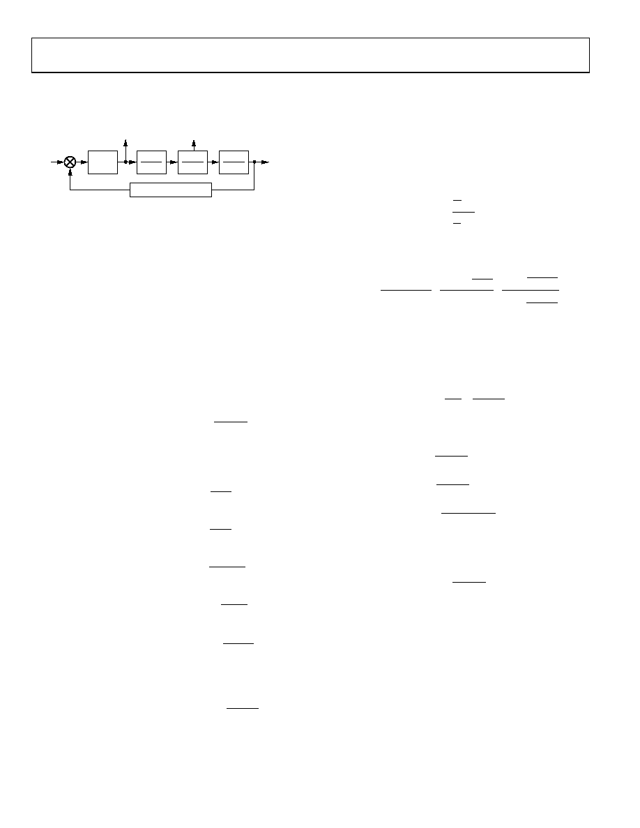
CIRCUIT DYNAMICS
AD2S1200 LOOP RESPONSE MODEL
04406-0-011
ERROR
(ACCELERATION)
–
θIN
θOUT
VELOCITY
k1
× k2
1–z –1
1–bz –1
1–z –1
c1–az –1
c
Sin/Cos LOOKUP
Figure 11. RDC System Response Block Diagram
The RDC is a mixed-signal device, which uses two A/D
converters to digitize signals from the resolver and a Type II
tracking loop to convert these to digital position and velocity
words.
The first gain stage consists of the ADC gain on the Sin/Cos
inputs, and the gain of the error signal into the first integrator.
The first integrator generates a signal proportional to velocity.
The compensation filter contains a pole and a zero, used to
provide phase margin and reduce high frequency noise gain.
The second integrator is the same as the first integrator and
generates the output position from the velocity signal. The
Sin/Cos lookup has unity gain. Values are given below for each
section:
ADC gain parameter
(k1nom = 1.8/2.5)
)
(
)
(
1
V
k
REF
p
IN
=
Error gain parameter
π
×
=
2
10
18
2
6
x
k
Compensator zero coefficient
4096
4095
=
a
Compensator pole coefficient
4096
4085
=
b
Integrator gain parameter
4096000
1
=
c
INT1 and INT2 transfer function
1
)
(
=
z
c
z
I
Compensation filter transfer
function
1
)
(
=
bz
az
z
C
R2D open-loop transfer function
)
(
)
(
2
1
)
(
2
z
C
z
I
k
z
G
×
=
R2D closed-loop transfer function
)
(
1
)
(
)
(
z
G
z
G
z
H
+
=
The closed-loop magnitude and phase responses are that of a
second-order low-pass filter (see Figure 12 and Figure 13).
To convert G(z) into the s-plane, we perform an inverse bilinear
transformation by substituting for z, where T = the sampling
period (1/4.096 MHz ≈ 244 ns).
s
T
s
T
z
+
=
2
Substitution yields the open-loop transfer function G(s).
)
1
(
2
)
1
(
1
)
1
(
2
)
1
(
1
4
1
)
1
(
2
1
)
(
2
b
T
s
a
T
s
T
s
sT
b
a
k
s
G
+
×
+
+
×
+
×
+
×
×
=
This transformation produces the best matching at low
frequencies (f << fSAMPLE). At lower frequencies (within the
closed-loop bandwidth of the AD2S1200), the transfer function
can be simplified to
2
1
2
1
)
(
st
s
K
s
G
a
+
×
where:
b
a
k
K
b
T
t
a
T
t
a
×
=
+
=
+
=
)
1
(
2
1
)
1
(
2
)
1
(
)
1
(
2
)
1
(
2
1
Solving for each value gives t1 = 1 s, t2 = 90 s, and Ka ≈ 7.4 ×
106 s
-2. Note that the closed-loop response is described as
)
(
1
)
(
)
(
s
G
s
G
s
H
+
=
By converting to the s-domain, we are able to quantify the
open-loop dc gain (Ka). This value is useful during calculation
of acceleration error of the loop as discussed in the Sources of
Error section.
The step response to a 10° input step is shown in Figure 14.
Because the error calculation (Equation 3) is nonlinear for large
values of θ , the response time for larger step changes in
position (90°–180°) will typically take three times as long as the
response to a small step change in position (<20°). In response
to a step change in velocity, the AD2S1200 will exhibit the same
response characteristics as for a step change in position.
相关PDF资料 |
PDF描述 |
|---|---|
| GEC10DRAI-S734 | CONN EDGECARD 20POS .100 R/A SLD |
| EBM25DCAI-S189 | CONN EDGECARD 50POS R/A .156 SLD |
| H6MMS-5018M | DIP CABLE - HDM50S/AE50M/HDM50S |
| A3CCH-1618M | IDC CABLE - AKC16H/AE16M/AKC16H |
| GBC10DRAH-S734 | CONN EDGECARD 20POS .100 R/A SLD |
相关代理商/技术参数 |
参数描述 |
|---|---|
| EVAL-AD2S1205CBZ | 制造商:Analog Devices 功能描述:EVALUATION BOARD I.C. |
| EVAL-AD2S1205SDZ | 功能描述:BOARD EVAL FOR AD2S1205 RoHS:是 类别:编程器,开发系统 >> 评估演示板和套件 系列:- 标准包装:1 系列:- 主要目的:电信,线路接口单元(LIU) 嵌入式:- 已用 IC / 零件:IDT82V2081 主要属性:T1/J1/E1 LIU 次要属性:- 已供物品:板,电源,线缆,CD 其它名称:82EBV2081 |
| EVAL-AD2S1210EDZ | 功能描述:BOARD EVAL AD2S1210 RoHS:是 类别:编程器,开发系统 >> 评估演示板和套件 系列:- 标准包装:1 系列:PSoC® 主要目的:电源管理,热管理 嵌入式:- 已用 IC / 零件:- 主要属性:- 次要属性:- 已供物品:板,CD,电源 |
| EVAL-AD4001FMCZ | 功能描述:EVAL BOARD FOR AD4001 制造商:analog devices inc. 系列:- 零件状态:在售 A/D 转换器数:1 位数:16 采样率(每秒):2M 数据接口:SPI,DSP 输入范围:±VREF 不同条件下的功率(典型值):20mW @ 2MSPS 使用的 IC/零件:AD4001 所含物品:板,电源 标准包装:1 |
| EVAL-AD421EB | 制造商:AD 制造商全称:Analog Devices 功能描述:Loop-Powered 4 mA to 20 mA DAC |
发布紧急采购,3分钟左右您将得到回复。