- 您现在的位置:买卖IC网 > PDF目录17075 > EVAL-AD5425EBZ (Analog Devices Inc)BOARD EVALUATION FOR AD5425 PDF资料下载
参数资料
| 型号: | EVAL-AD5425EBZ |
| 厂商: | Analog Devices Inc |
| 文件页数: | 13/25页 |
| 文件大小: | 0K |
| 描述: | BOARD EVALUATION FOR AD5425 |
| 产品培训模块: | DAC Architectures |
| 标准包装: | 1 |
| DAC 的数量: | 1 |
| 位数: | 8 |
| 采样率(每秒): | 2.47M |
| 数据接口: | 串行 |
| 设置时间: | 15ns |
| DAC 型: | 电流 |
| 工作温度: | -40°C ~ 125°C |
| 已供物品: | 板,CD |
| 已用 IC / 零件: | AD5425 |
| 相关产品: | AD5425YRMZ-REEL7-ND - IC DAC 8BIT MULTIPLYING 10MSOP AD5425YRMZ-REEL-ND - IC DAC 8BIT MULTIPLYING 10MSOP AD5425YRMZ-ND - IC DAC 8BIT MULTIPLYING 10MSOP AD5425YRM-REEL7-ND - IC DAC 8BIT MULTIPLYING 10-MSOP AD5425YRM-REEL-ND - IC DAC 8BIT MULTIPLYING 10-MSOP AD5425YRM-ND - IC DAC MULTIPLYING 8BIT 10-MSOP |
Data Sheet
AD5425
Rev. C | Page 19 of 24
SERIAL INTERFACE
The AD5425 has a simple 3-wire interface that is compatible
with SPI, QSPI, MICROWIRE, and DSP interface standards.
Data is written to the device in 8-bit words. This 8-bit word
consists of 8 data bits, as shown in Figure 37.
Figure 37. 8-Bit Input Shift Register Contents
SYNC is an edge-triggered input that acts as a frame synchro-
nization signal and chip enable. Data can be transferred into the
device only while SYNC is low. To start the serial data
transfer, SYNC should be taken low, observing the
minimum SYNC falling to SCLK falling edge setup time, t4.
After loading eight data bits to the shift register, the SYNC line
is brought high. The contents of the DAC register and the
output are updated by bringing LDAC low any time after the
8-bit data transfer is complete, as seen in the timing diagram of
Figure 2. LDAC can be tied permanently low if required. For
another serial transfer to take place, the interface must be
enabled by another falling edge of SYNC.
Low Power Serial Interface
To minimize the power consumption of the device, the interface
fully powers up only when the device is being written to, that is,
on the falling edge of SYNC. The SCLK and SDIN input buffers
are powered down on the rising edge of SYNC.
MICROPROCESSOR INTERFACING
Microprocessor interfacing to this DAC is via a serial bus that
uses standard protocol compatible with microcontrollers and
DSP processors. The communications channel is a 3-wire inter-
face consisting of a clock signal, a data signal, and a synchro-
nization signal. An LDAC pin is also included. The AD5425
requires an 8-bit word with the default being data valid on the
falling edge of SCLK, but this is changeable via the control bits
in the data-word.
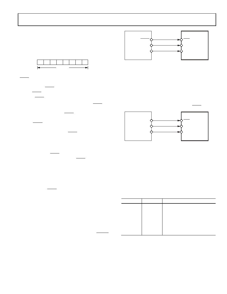
ADSP-21xx-to AD5425 Interface
The ADSP-21xx family of DSPs is easily interfaced to this
family of DACs without extra glue logic. Figure 38 shows
an example of an SPI interface between the DAC and the
ADSP-2191M. SCK of the DSP drives the serial data line, DIN.
SYNC is driven from one of the port lines, in this case SPIxSEL.
Figure 38. ADSP-2191M SPI-to-AD5425 Interface
A serial interface between the DAC and DSP SPORT is shown
in Figure 39. In this interface example, SPORT0 is used to
transfer data to the DAC shift register. Transmission is initiated
by writing a word to the Tx register after the SPORT has been
enabled. In a write sequence, data is clocked out on each rising
edge of the DSP’s serial clock and clocked into the DAC input
shift register on the falling edge of its SCLK. The update of the
DAC output takes place on the rising edge of the SYNC signal.
Figure 39. ADSP-2101/ADSP-2191M SPORT-to-AD5425 Interface
Communication between two devices at a given clock speed is
possible when the following specifications from one device to
the other are compatible: frame sync delay and frame sync setup
and hold, data delay and data setup and hold, and SCLK width.
The DAC interface expects a t4 (SYNC falling edge to SCLK
falling edge setup time) of 13 ns minimum. Consult the ADSP-
21xx user manual for information on clock and frame sync
frequencies for the SPORT register.
Table 10. SPORT Control Register Setup
Name
Setting
Description
TFSW
1
Alternate framing
INVTFS
1
Active low frame signal
DTYPE
00
Right-justify data
ISCLK
1
Internal serial clock
TFSR
1
Frame every word
ITFS
1
Internal framing signal
SLEN
0111
8-bit data-word
DB0 (LSB)
DB7 (MSB)
DB7 DB6 DB5 DB4 DB3 DB2
DB0
DB1
DATA BITS
03161-037
SCLK
SCK
AD54251
SPIxSEL
SDIN
MOSI
ADSP-2191M1
03161-
038
1 ADDITIONAL PINS OMITTED FOR CLARITY.
SYNC
03161-
039
SCLK
AD54251
SYNC
TFS
SDIN
DT
ADSP-2101/
ADSP-2191M1
1 ADDITIONAL PINS OMITTED FOR CLARITY.
相关PDF资料 |
PDF描述 |
|---|---|
| VI-B5K-EY | CONVERTER MOD DC/DC 40V 50W |
| V375C2E50BL3 | CONVERTER MOD DC/DC 2V 50W |
| VI-B4R-EY | CONVERTER MOD DC/DC 7.5V 50W |
| VI-B4M-EY | CONVERTER MOD DC/DC 10V 50W |
| V375C2E50BL2 | CONVERTER MOD DC/DC 2V 50W |
相关代理商/技术参数 |
参数描述 |
|---|---|
| EVAL-AD5426EB | 制造商:Analog Devices 功能描述:EVAL BD FOR AD5426, 0BIT HIGH BANDWIDTH MULTIPLYING DACS W/ - Bulk |
| EVAL-AD5428EBZ | 制造商:Analog Devices 功能描述:EVAL BD FOR 8-/10-/12-BIT, PARALLEL INPUT, DUAL-CH, CURRENT - Bulk |
| EVAL-AD5429EB | 制造商:Analog Devices 功能描述:EVALUATION BOARD I.C. - Bulk |
| EVAL-AD5429EBZ | 制造商:Analog Devices 功能描述:Evaluation Board Dual 8/10/12Bit, High Bandwidth, Multiplying DACs With Serial Interface 制造商:Analog Devices 功能描述:EVAL BD DUAL 8-/10-/12-BIT, HIGH BANDWIDTH, MULTIPLYING DACS - Bulk |
| EVAL-AD5432EB | 制造商:Analog Devices 功能描述:EVAL BD FOR AD5432, 0BIT HIGH BANDWIDTH MULTIPLYING DACS W/ - Bulk |
发布紧急采购,3分钟左右您将得到回复。