- 您现在的位置:买卖IC网 > PDF目录17030 > EVAL-AD7706EBZ (Analog Devices Inc)BOARD EVALUATION FOR AD7706 PDF资料下载
参数资料
| 型号: | EVAL-AD7706EBZ |
| 厂商: | Analog Devices Inc |
| 文件页数: | 15/44页 |
| 文件大小: | 0K |
| 描述: | BOARD EVALUATION FOR AD7706 |
| 标准包装: | 1 |
| ADC 的数量: | 1 |
| 位数: | 16 |
| 采样率(每秒): | 500 |
| 数据接口: | 串行 |
| 输入范围: | 0 ~ 5.25 V |
| 在以下条件下的电源(标准): | 6.5mW @ 500SPS |
| 工作温度: | -40°C ~ 85°C |
| 已用 IC / 零件: | AD7706 |
| 已供物品: | 板,CD |
| 相关产品: | AD7706BNZ-ND - IC ADC 16BIT 3CHAN 16DIP AD7706BRUZ-REEL7-ND - IC ADC 16BIT 3CHAN 16TSSOP AD7706BRZ-REEL7TR-ND - IC ADC 16BIT 3CHAN 16SOIC AD7706BRUZ-REEL-ND - IC ADC 16BIT 3CHAN 16TSSOP AD7706BRZ-REEL-ND - IC ADC 16BIT 3CHAN 16SOIC AD7706BRZ-ND - IC ADC 16BIT 3CH 16-SOIC AD7706BRUZ-ND - IC ADC 16BIT 3CH 16-TSSOP AD7706BRU-REEL7-ND - IC ADC 16BIT 3CH 16-TSSOP T/R AD7706BRU-ND - IC ADC 16BIT 3CH 16-TSSOP AD7706BR-REEL7-ND - IC ADC 16BIT 3CH 16-SOIC T/R 更多... |
第1页第2页第3页第4页第5页第6页第7页第8页第9页第10页第11页第12页第13页第14页当前第15页第16页第17页第18页第19页第20页第21页第22页第23页第24页第25页第26页第27页第28页第29页第30页第31页第32页第33页第34页第35页第36页第37页第38页第39页第40页第41页第42页第43页第44页
AD7705/AD7706
Rev. C | Page 22 of 44
ANALOG INPUT
Ranges
The AD7705 contains two differential analog input pairs,
AIN1(+)/AIN1() and AIN2(+)/AIN2(). These input pairs
provide programmable-gain, differential input channels that can
handle either unipolar or bipolar input signals. It should be noted
that the bipolar input signals are referenced to the respective
AIN() input of each input pair. The AD7706 contains three
pseudo differential analog input pairs, AIN1, AIN2, and AIN3,
which are referenced to the COMMON input.
In unbuffered mode, the common-mode range of the input is
from GND to VDD, provided that the absolute value of the analog
input voltage lies between GND 100 mV and VDD + 30 mV.
Therefore, in unbuffered mode, the part can handle both unipolar
and bipolar input ranges for all gains. The AD7705 can tolerate
absolute analog input voltages down to GND 200 mV, but the
leakage current increases at high temperatures. In buffered mode,
the analog inputs can handle much larger source impedances,
but the absolute input voltage range is restricted to between
GND + 50 mV and VDD 1.5 V, which also restricts the common-
mode range. Therefore, in buffered mode, there are some
restrictions on the allowable gains for bipolar input ranges. Care
must be taken in setting up the common-mode voltage and
input voltage ranges so that the above limits are not exceeded;
otherwise, there is a degradation in linearity performance.
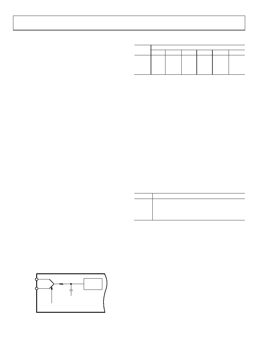
In unbuffered mode, the analog inputs look directly into the
7 pF input sampling capacitor, CSAMP. The dc input leakage
current in this unbuffered mode is 1 nA maximum. As a result,
the analog inputs see a dynamic load that is switched at the
input sample rate (see Figure 14). This sample rate depends on
master clock frequency and selected gain. CSAMP is charged to
AIN(+) and discharged to AIN() every input sample cycle.
The effective on resistance of the switch, RSW, is typically 7 kΩ.
CSAMP must be charged through RSW and any external source
impedances every input sample cycle. Therefore, in unbuffered
mode, source impedances mean a longer charge time for CSAMP,
which might result in gain errors on the parts. Table 22 shows
the allowable external resistance-capacitance values for unbuffered
mode, such that no gain error to the 16-bit level is introduced in
the part. Note that these capacitances are total capacitances on
the analog input—external capacitance plus 10 pF capacitance
from the pins and lead frame of the devices.
AIN(+)
AIN(–)
SWITCHING FREQUENCY DEPENDS ON
fCLKIN AND SELECTED GAIN
RSW (7kΩ TYP)
CSAMP
(7pF)
HIGH
IMPEDANCE
>1G
VBIAS
01166-014
Figure 14. Unbuffered Analog Input Structure
Table 22. External Resistance-Capacitance Combination for
Unbuffered Mode (Without 16-Bit Gain Error)
External Capacitance (pF)
Gain
10
50
100
500
1000
5000
1
152 kΩ
53.9 kΩ
31.4 kΩ
8.4 kΩ
4.76 kΩ
1.36 kΩ
2
75.1 kΩ
26.6 kΩ
15.4 kΩ
4.14 kΩ
2.36 kΩ
670 Ω
4
34.2 kΩ
12.77 kΩ
7.3 kΩ
1.95 kΩ
1.15 kΩ
320 Ω
8 to 128
16.7 kΩ
5.95 kΩ
3.46 kΩ
924 Ω
526 Ω
150 Ω
In buffered mode, the analog inputs look into the high impedance
inputs stage of the on-chip buffer amplifier. CSAMP is charged via
this buffer amplifier such that source impedances do not affect
the charging of CSAMP. This buffer amplifier has an offset leakage
current of 1 nA. In this buffered mode, large source impedances
result in a small dc offset voltage developed across the source
impedance, but not in a gain error.
Sample Rate
The modulator sample frequency for the AD7705/AD7706
remains at fCLKIN/128 (19.2 kHz @ fCLKIN = 2.4576 MHz), regardless
of the selected gain. However, gains greater than 1 are achieved
by a combination of multiple input samples per modulator cycle
and a scaling of the ratio of reference capacitor to input capacitor.
As a result of the multiple sampling, the input sample rate of
these devices varies with the selected gain (see Table 23). In
buffered mode, the input is buffered before the input sampling
capacitor. In unbuffered mode, where the analog input looks
directly into the sampling capacitor, the effective input impedance
is 1/CSAMP × fS, where CSAMP is the input sampling capacitance
and fS is the input sample rate.
Table 23. Input Sampling Frequency vs. Gain
Gain
Input Sampling Frequency (fS)
1
fCLKIN/64 (38.4 kHz @ fCLKIN = 2.4576 MHz)
2
2 × fCLKIN/64 (76.8 kHz @ fCLKIN = 2.4576 MHz)
4
4 × fCLKIN/64 (76.8 kHz @ fCLKIN = 2.4576 MHz)
8 to 128
8 × fCLKIN/64 (307.2 kHz @ fCLKIN = 2.4576 MHz)
BIPOLAR/UNIPOLAR INPUT
The analog inputs on the AD7705/AD7706 can accept either
unipolar or bipolar input voltage ranges. Bipolar input ranges
do not imply that these parts can handle negative voltages on
their analog inputs; the analog inputs cannot go more negative
than 100 mV to ensure correct operation of these parts. The
input channels are fully differential. As a result, on the AD7705,
the voltage to which the unipolar and bipolar signals on the
AIN(+) input are referenced is the voltage on the respective
AIN() input.
相关PDF资料 |
PDF描述 |
|---|---|
| SDS130R-473M | INDUCTOR PWR SHIELDED 47UH SMD |
| ECM10DKKI | CONN EDGECARD 20POS .156 WW |
| EBC18DRYN-S93 | CONN EDGECARD 36POS DIP .100 SLD |
| VI-B7K-EY | CONVERTER MOD DC/DC 40V 50W |
| RYM06DTKN-S288 | CONN EDGECARD 12POS .156 EXTEND |
相关代理商/技术参数 |
参数描述 |
|---|---|
| EVAL-AD7707EB | 制造商:Analog Devices 功能描述:EVAL KIT FOR 3V/5 V, 610 V INPUT RANGE, 1 MW 3-CH 16BIT, SIG - Bulk |
| EVAL-AD7708EB | 制造商:Analog Devices 功能描述:EVALUATION BOARD I.C. - Bulk |
| EVAL-AD7708EBZ | 功能描述:BOARD EVAL FOR AD7708 RoHS:是 类别:编程器,开发系统 >> 评估板 - 模数转换器 (ADC) 系列:- 产品培训模块:Obsolescence Mitigation Program 标准包装:1 系列:- ADC 的数量:1 位数:12 采样率(每秒):94.4k 数据接口:USB 输入范围:±VREF/2 在以下条件下的电源(标准):- 工作温度:-40°C ~ 85°C 已用 IC / 零件:MAX11645 已供物品:板,软件 |
| EVAL-AD7709EB | 制造商:Analog Devices 功能描述:EVAL KIT FOR 16BIT- ADC W/ SWITABLE CURRENT SOURCES - Bulk |
| EVAL-AD7710EB | 制造商:AD 制造商全称:Analog Devices 功能描述:Signal Conditioning ADC |
发布紧急采购,3分钟左右您将得到回复。