- 您现在的位置:买卖IC网 > PDF目录17030 > EVAL-AD7731EBZ (Analog Devices Inc)BOARD EVALUATION FOR AD7731 PDF资料下载
参数资料
| 型号: | EVAL-AD7731EBZ |
| 厂商: | Analog Devices Inc |
| 文件页数: | 18/44页 |
| 文件大小: | 0K |
| 描述: | BOARD EVALUATION FOR AD7731 |
| 标准包装: | 1 |
| ADC 的数量: | 1 |
| 位数: | 24 |
| 采样率(每秒): | 6.4k |
| 数据接口: | 串行 |
| 输入范围: | ±1.28 V |
| 在以下条件下的电源(标准): | 67.5mW @ 6.4kSPS |
| 工作温度: | -40°C ~ 85°C |
| 已用 IC / 零件: | AD7731 |
| 已供物品: | 板,CD |
| 相关产品: | AD7731BNZ-ND - IC ADC 24BIT SIGMA-DELTA 24DIP AD7731BRUZ-REEL7-ND - IC ADC 24BIT SIGMA-DELTA 24TSSOP AD7731BRUZ-REEL-ND - IC ADC 24BIT SIGMA-DELTA 24TSSOP AD7731BRUZ-ND - IC ADC 24BIT SIGMA-DELTA 24TSSOP AD7731BRZ-REEL7-ND - IC ADC 24BIT SIGMA-DELTA 24-SOIC AD7731BRZ-REEL-ND - IC ADC 24BIT SIGMA-DELTA 24-SOIC AD7731BRZ-ND - IC ADC 24BIT SIGMA-DELTA 24-SOIC AD7731BRU-REEL7-ND - IC ADC 24BIT SIGMA-DELTA 24TSSOP AD7731BRU-ND - IC ADC 24BIT SIGMA-DELTA 24TSSOP AD7731BR-REEL7-ND - IC ADC 24BIT SIGMA-DELTA 24-SOIC 更多... |
第1页第2页第3页第4页第5页第6页第7页第8页第9页第10页第11页第12页第13页第14页第15页第16页第17页当前第18页第19页第20页第21页第22页第23页第24页第25页第26页第27页第28页第29页第30页第31页第32页第33页第34页第35页第36页第37页第38页第39页第40页第41页第42页第43页第44页
AD7731
–25–
REV. 0
The operation mode can be changed to achieve optimum per-
formance in various applications. The CHP bit should generally
be set to 0 when using the AD7731 in applications where higher
throughput rates are a concern or in applications where the
reduced rejection at the chopping frequency in chop mode is an
issue. The part should be operated with CHP = 1 when drift,
noise rejection and optimum EMI rejection are important crite-
ria in the application.
The output update rate of the AD7731 is programmed using the
SF bits of the Filter Register. With CHP = 0, the output update
is determined by the relationship:
Output Rate
= f
MOD ×
1
SF
CHP
= 0
()
where SF is the decimal equivalent of the data loaded to the SF
bits of the Filter Register and fMOD is the modulator frequency
and is 1/16th of the master clock frequency.
With CHP = 1, the output update is determined by the relation-
ship:
Output Rate
= f
MOD ×
1
3
× SF
CHP
= 1
()
where SF is the decimal equivalent of the data loaded to the SF
bits of the Filter Register and fMOD is the modulator frequency
and is 1/16th of the master clock frequency.
Thus for a given SF word the output rate from the AD7731 is
three times faster with CHP = 0 than CHP = 1.
The various filter stages and options are discussed in the follow-
ing sections.
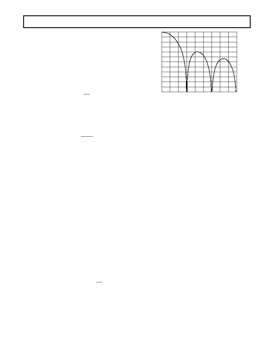
First Stage Filter/SKIP Mode Enabled (SKIP = 1)
With SKIP mode enabled, the only filtering on the part is the
first stage filter. The frequency response for this first stage filter
is shown in Figure 8. The response of this first stage filter is
similar to that of an averaging filter but with a sharper roll-off.
With CHP = 0, the output rate for the filter corresponds with
the positioning of the first notch of the filter’s frequency re-
sponse. Thus, for the plot of Figure 8 where the output rate is
600 Hz (fCLK IN = 4.9152 MHz and SF = 512), the first notch of
the filter is at 600 Hz. With CHP = 1, the magnitude response
is the same as in Figure 8 but in this case, the output rate is
1/3rd the output rate so for the example shown in Figure 8 the
output data rate is 200 Hz. The notches of this sinc
3 filter fre-
quency response are repeated at multiples of the first notch. The
filter provides attenuation of better than 100 dB around these
notches. Programming a different cutoff frequency via SF0 –
SF11 does not alter the profile of the filter response; it simply
changes the location of the notches. The –3 dB frequency for both
Chop and Nonchop modes is defined as:
f
3 dB = 0. 262 × f MOD ×
1
SF
Nonchop Mode (SKIP = 1, CHP = 0)
With CHP = 0, the input chopping on the AD7731 is disabled
and any offset content in the samples to the first stage filter are
all of the same polarity. When using the part in SKIP mode, the
user can take the output from the AD7731 directly. Time to the
first output for the part is 3
× 1/Output Rate in this mode. Table
XVIII summarizes the settling time and subsequent throughput
rate for the various different modes.
FREQUENCY – Hz
0
–60
–100
0
1800
GAIN
–
dB
200
400
600
800
1000
1200
1400
1600
–10
–50
–70
–90
–30
–40
–80
–20
–120
–110
Figure 8. SKIP Mode Frequency Response (SKIP = 1,
SF = 512)
Chop Mode (SKIP = 1, CHP = 1)
With CHP = 1, the AD7731 alternatively reverses the ADC
inputs, producing an output which contains the channel offset
when not reversed and the negative of the offset when reversed.
As a result, when operating in SKIP mode, the user has to take
two subsequent outputs from the AD7731 and average them to
produce a valid output from the first stage filter. While operat-
ing in this mode gives the benefits of chopping without the
longer settling time associated with the 22-tap FIR filter, care
should be taken with input signals near positive full-scale or
negative full-scale (zero-scale in unipolar mode). Since the
calibration coefficients are generated for the averaged offset, and
not for the individual offsets represented in each sample, one of
the two samples in the pair may record an all 1s or all 0s read-
ing. If this happens it will result in an error in the averaged
reading. Time to first output for the part is 1/Output Rate in
this mode. However, since the user really needs two outputs to
derive a correct chopped result, the time to get two outputs for
averaging is 2
× 1/Output Rate. Table XVIII summarizes the
settling time and subsequent throughput rate for the various
different modes. If the user wants the benefits of chopping with-
out the longer settling time associated with the 22-tap FIR filter,
it is recommended that the part be used in FASTStep mode.
Second Stage Filter
With SKIP mode disabled, the second stage filter is included in
the signal processing. This second stage filter produces a differ-
ent response depending on the CHP and FAST bits.
Normal FIR Operation (SKIP = 0)
The normal mode of operation of the second stage filter is as a
22-tap low-pass FIR filter. This second stage filter processes the
output of the first stage filter and the net frequency response of
the filter is simply a product of the filter response of both filters.
The overall filter response of the AD7731 is guaranteed to have
no overshoot.
REV. A
相关PDF资料 |
PDF描述 |
|---|---|
| VI-B7J-EY | CONVERTER MOD DC/DC 36V 50W |
| RMM06DTKN-S288 | CONN EDGECARD 12POS .156 EXTEND |
| VI-B7H-EY | CONVERTER MOD DC/DC 52V 50W |
| SDS130R-302N | INDUCTOR PWR SHIELDED 3.0UH SMD |
| VI-B74-EY | CONVERTER MOD DC/DC 48V 50W |
相关代理商/技术参数 |
参数描述 |
|---|---|
| EVAL-AD7732EB | 制造商:Analog Devices 功能描述:2-CHANNEL, ??10 V INPUT RANGE, HIGH THROUGHPUT, 24-BIT ADC |
| EVAL-AD7732EBZ | 功能描述:BOARD EVAL FOR AD7732 RoHS:是 类别:编程器,开发系统 >> 评估板 - 模数转换器 (ADC) 系列:- 产品培训模块:Obsolescence Mitigation Program 标准包装:1 系列:- ADC 的数量:1 位数:12 采样率(每秒):94.4k 数据接口:USB 输入范围:±VREF/2 在以下条件下的电源(标准):- 工作温度:-40°C ~ 85°C 已用 IC / 零件:MAX11645 已供物品:板,软件 |
| EVAL-AD7734EBZ | 功能描述:BOARD EVALUATION FOR AD7734 RoHS:是 类别:编程器,开发系统 >> 评估板 - 模数转换器 (ADC) 系列:- 产品培训模块:Obsolescence Mitigation Program 标准包装:1 系列:- ADC 的数量:1 位数:12 采样率(每秒):94.4k 数据接口:USB 输入范围:±VREF/2 在以下条件下的电源(标准):- 工作温度:-40°C ~ 85°C 已用 IC / 零件:MAX11645 已供物品:板,软件 |
| EVAL-AD7738EB | 制造商:Analog Devices 功能描述:Evaluation Board For AD7738 ADC 制造商:Analog Devices 功能描述:EVALUATION BOARD I.C. - Bulk |
| EVAL-AD7738EBZ | 功能描述:BOARD EVAL FOR AD7738 RoHS:是 类别:编程器,开发系统 >> 评估板 - 模数转换器 (ADC) 系列:- 产品培训模块:Obsolescence Mitigation Program 标准包装:1 系列:- ADC 的数量:1 位数:12 采样率(每秒):94.4k 数据接口:USB 输入范围:±VREF/2 在以下条件下的电源(标准):- 工作温度:-40°C ~ 85°C 已用 IC / 零件:MAX11645 已供物品:板,软件 |
发布紧急采购,3分钟左右您将得到回复。