- 您现在的位置:买卖IC网 > PDF目录17050 > EVAL-AD7760EDZ (Analog Devices Inc)BOARD EVAL CONTROL AD7760 PDF资料下载
参数资料
| 型号: | EVAL-AD7760EDZ |
| 厂商: | Analog Devices Inc |
| 文件页数: | 14/37页 |
| 文件大小: | 0K |
| 描述: | BOARD EVAL CONTROL AD7760 |
| 标准包装: | 1 |
| ADC 的数量: | 1 |
| 位数: | 24 |
| 采样率(每秒): | 2.5M |
| 数据接口: | 并联 |
| 输入范围: | ±3.25 Vpp |
| 在以下条件下的电源(标准): | 958mW @ 2.5MSPS |
| 工作温度: | -40°C ~ 85°C |
| 已用 IC / 零件: | AD7760 |
| 已供物品: | 板,CD |
第1页第2页第3页第4页第5页第6页第7页第8页第9页第10页第11页第12页第13页当前第14页第15页第16页第17页第18页第19页第20页第21页第22页第23页第24页第25页第26页第27页第28页第29页第30页第31页第32页第33页第34页第35页第36页第37页
AD7760
Rev. A | Page 20 of 36
MODULATOR DATA OUTPUT MODE INTERFACE
The AD7760 can be configured in modulator data output mode
(bypassing the default decimation filtering) by writing 0 to each
of the bits contained in Control Register 1: BYP F1, BYP F3,
and DEC [2:0]. This will bypass all digital decimation filtering
offered by the AD7760. See the AD7760 Registers section for
further details.
When the AD7760 is operating in modulator data output mode,
a different parallel interfacing scheme than that used for config-
urations, where the AD7760’s data output is filtered is necessary.
The data output rate depends on the clock divider ratio that is
used. When the CDIV bit in Control Register 2 is set to logic
high, data is output at the MCLK frequency. If the CDIV bit is
set to logic low, data is output at a frequency of MCLK/2. See
the Clocking the AD7760 section.
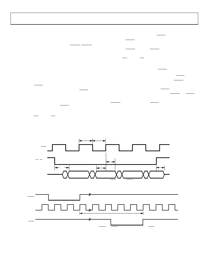
CLOCK DIVIDE-BY-1 MODE (CDIV = 1)
When obtaining data from the AD7760 in modulator output
mode, both the RD/WR and CS lines must be held low. This
brings the data bus out of its high impedance state. Figure 43
shows the timing diagram for reading data in the modulator data
output mode when operating with CDIV = 1 (that is, ICLK =
MCLK). A DRDY pulse is generated for each word. The data on
each of the 16 data output pins, D [15:0], is valid on the rising
edge of the DRDY pulse. The DRDY pulse can be used to latch
the modulator data into a FIFO or as a DMA control signal. Shortly
after the RD/WR and CS lines return high, the AD7760 stops
outputting data and the data bus returns to high impedance.
CLOCK DIVIDE-BY-2 MODE (CDIV = 0)
When operating in modulator output mode with CDIV = 0
(that is, ICLK = MCLK/2), the frequency of the DRDY signal
created is half that of the MCLK frequency input to the device.
The timing scheme that is used when CDIV = 0 depends on the
number of MCLK cycles that occur between RESET and SYNC.
If the number of MCLK cycles (n) between the rising edge of
RESET and the rising edge of SYNC (see Figure 44) is an even
value, use the interface timing shown in Figure 43. If n is an odd
value, use the interface timing shown in Figure 45.
t9
t10
t14
t11
t12
t13
DRDY
CS, RD/WR
D[0:15]
INVALID DATA
MOD DATA M
MOD DATA M + 1
MOD D...
04
97
5-
0
50
Figure 43. AD7760 Modulator Output Mode (CDIV = 1) and (CDIV = 0, n is even)
MCLK
RESET
SYNC
n×
tMCLK
04
975
-05
1
Figure 44. AD7760 Relative Timing Between RESET and SYNC in Modulator Output Mode CDIV = 0
相关PDF资料 |
PDF描述 |
|---|---|
| GCM22DCMD | CONN EDGECARD 44POS .156 WW |
| REC5-4815DRW/H2/C | CONV DC/DC 5W 36-72VIN +/-15VOUT |
| ISL5861EVAL2 | EVALUATION PLATFORM ISL5861 TSSO |
| REC5-4815DRW/H2/A | CONV DC/DC 5W 36-72VIN +/-15VOUT |
| GCA18DTMN | CONN EDGECARD 36POS R/A .125 SLD |
相关代理商/技术参数 |
参数描述 |
|---|---|
| EVAL-AD7762EB | 制造商:Analog Devices 功能描述:EVALUATION CONTROL BOARD I.C. - Bulk |
| EVAL-AD7762EBZ | 制造商:Analog Devices 功能描述:EVALUATION CONTROL BOARD I.C. - Bulk |
| EVAL-AD7762EDZ | 功能描述:BOARD EVAL CONTROL AD7762 RoHS:是 类别:编程器,开发系统 >> 评估板 - 模数转换器 (ADC) 系列:- 产品培训模块:Obsolescence Mitigation Program 标准包装:1 系列:- ADC 的数量:1 位数:12 采样率(每秒):94.4k 数据接口:USB 输入范围:±VREF/2 在以下条件下的电源(标准):- 工作温度:-40°C ~ 85°C 已用 IC / 零件:MAX11645 已供物品:板,软件 |
| EVAL-AD7763EB | 制造商:Analog Devices 功能描述:EVALUATION BOARD I.C. - Bulk |
| EVAL-AD7763EBZ | 制造商:Analog Devices 功能描述:EVALUATION BOARD I.C. - Bulk |
发布紧急采购,3分钟左右您将得到回复。