- 您现在的位置:买卖IC网 > PDF目录17050 > EVAL-AD7760EDZ (Analog Devices Inc)BOARD EVAL CONTROL AD7760 PDF资料下载
参数资料
| 型号: | EVAL-AD7760EDZ |
| 厂商: | Analog Devices Inc |
| 文件页数: | 15/37页 |
| 文件大小: | 0K |
| 描述: | BOARD EVAL CONTROL AD7760 |
| 标准包装: | 1 |
| ADC 的数量: | 1 |
| 位数: | 24 |
| 采样率(每秒): | 2.5M |
| 数据接口: | 并联 |
| 输入范围: | ±3.25 Vpp |
| 在以下条件下的电源(标准): | 958mW @ 2.5MSPS |
| 工作温度: | -40°C ~ 85°C |
| 已用 IC / 零件: | AD7760 |
| 已供物品: | 板,CD |
第1页第2页第3页第4页第5页第6页第7页第8页第9页第10页第11页第12页第13页第14页当前第15页第16页第17页第18页第19页第20页第21页第22页第23页第24页第25页第26页第27页第28页第29页第30页第31页第32页第33页第34页第35页第36页第37页
AD7760
Rev. A | Page 21 of 36
INVALID DATA
MOD DATA M
MOD DATA M + 1
MOD D...
t9
t10
t20
DRDY
D[0:15]
MCLK
CS, RD/WR
t11
t19
t14
0
497
5-
0
52
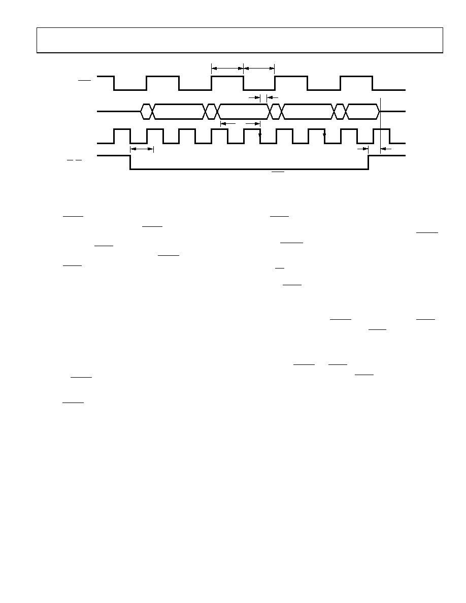
Figure 45. AD7760 Modulator Output Mode (CDIV = 0, n is odd)
In the case where n is an odd number of MCLK cycles, the
modulator data output on Pins D [15:0] is output on the rising
edge of DRDY. In this case, the modulator data should be read
on the falling edge of MCLK when DRDY is logic low. Figure 45
shows timing details to be used when reading the modulator
output data where CDIV = 0 and there is an odd number of
MCLK cycles between the rising edge of RESET and the rising
edge of SYNC. The edge of MCLK that should be used under
these conditions is illustrated in Figure 45 by arrows on the
MCLK falling edges in question.
USING THE AD7760
IN MODULATOR OUTPUT MODE
The following is the recommended sequence for powering up
and using the AD7760:
1.
Apply power.
2.
Start the clock oscillator, applying MCLK.
3.
Take RESET low for a minimum of one MCLK cycle.
4.
Wait a minimum of two MCLK cycles after the rising edge
of RESET.
5.
Write to Control Register 2 to power up the ADC and the
differential amplifier as required. The correct clock divider
(CDIV) ratio should be programmed at this time.
6.
Write to Control Register 1 to set the bypass filter bits, BYP F1
and BYP F3, and the decimation rate bits, DEC [2:0], to 0.
7.
Wait a minimum of six MCLK cycles after the rising edge
of CS has been released.
8.
Take SYNC low for a minimum of four MCLK cycles, if
required, to synchronize multiple parts.
Using this sequence results in an even number of MCLK cycles
between the rising edge of RESET and the rising edge of SYNC.
Therefore, when using this sequence with CDIV = 0, the interface
timing shown in Figure 43 should be implemented.
Note that whether the number of MCLK cycles between the
rising edge of RESET and SYNC is odd or even is irrelevant
when the AD7760 is operated with CDIV = 1.
When using the AD7760 in modulator output mode, the offset,
gain, and overrange registers are not operational. The only
registers that can be used are Control Register 1 and Control
Register 2.
相关PDF资料 |
PDF描述 |
|---|---|
| GCM22DCMD | CONN EDGECARD 44POS .156 WW |
| REC5-4815DRW/H2/C | CONV DC/DC 5W 36-72VIN +/-15VOUT |
| ISL5861EVAL2 | EVALUATION PLATFORM ISL5861 TSSO |
| REC5-4815DRW/H2/A | CONV DC/DC 5W 36-72VIN +/-15VOUT |
| GCA18DTMN | CONN EDGECARD 36POS R/A .125 SLD |
相关代理商/技术参数 |
参数描述 |
|---|---|
| EVAL-AD7762EB | 制造商:Analog Devices 功能描述:EVALUATION CONTROL BOARD I.C. - Bulk |
| EVAL-AD7762EBZ | 制造商:Analog Devices 功能描述:EVALUATION CONTROL BOARD I.C. - Bulk |
| EVAL-AD7762EDZ | 功能描述:BOARD EVAL CONTROL AD7762 RoHS:是 类别:编程器,开发系统 >> 评估板 - 模数转换器 (ADC) 系列:- 产品培训模块:Obsolescence Mitigation Program 标准包装:1 系列:- ADC 的数量:1 位数:12 采样率(每秒):94.4k 数据接口:USB 输入范围:±VREF/2 在以下条件下的电源(标准):- 工作温度:-40°C ~ 85°C 已用 IC / 零件:MAX11645 已供物品:板,软件 |
| EVAL-AD7763EB | 制造商:Analog Devices 功能描述:EVALUATION BOARD I.C. - Bulk |
| EVAL-AD7763EBZ | 制造商:Analog Devices 功能描述:EVALUATION BOARD I.C. - Bulk |
发布紧急采购,3分钟左右您将得到回复。