- 您现在的位置:买卖IC网 > PDF目录17050 > EVAL-AD7760EDZ (Analog Devices Inc)BOARD EVAL CONTROL AD7760 PDF资料下载
参数资料
| 型号: | EVAL-AD7760EDZ |
| 厂商: | Analog Devices Inc |
| 文件页数: | 21/37页 |
| 文件大小: | 0K |
| 描述: | BOARD EVAL CONTROL AD7760 |
| 标准包装: | 1 |
| ADC 的数量: | 1 |
| 位数: | 24 |
| 采样率(每秒): | 2.5M |
| 数据接口: | 并联 |
| 输入范围: | ±3.25 Vpp |
| 在以下条件下的电源(标准): | 958mW @ 2.5MSPS |
| 工作温度: | -40°C ~ 85°C |
| 已用 IC / 零件: | AD7760 |
| 已供物品: | 板,CD |
第1页第2页第3页第4页第5页第6页第7页第8页第9页第10页第11页第12页第13页第14页第15页第16页第17页第18页第19页第20页当前第21页第22页第23页第24页第25页第26页第27页第28页第29页第30页第31页第32页第33页第34页第35页第36页第37页
AD7760
Rev. A | Page 27 of 36
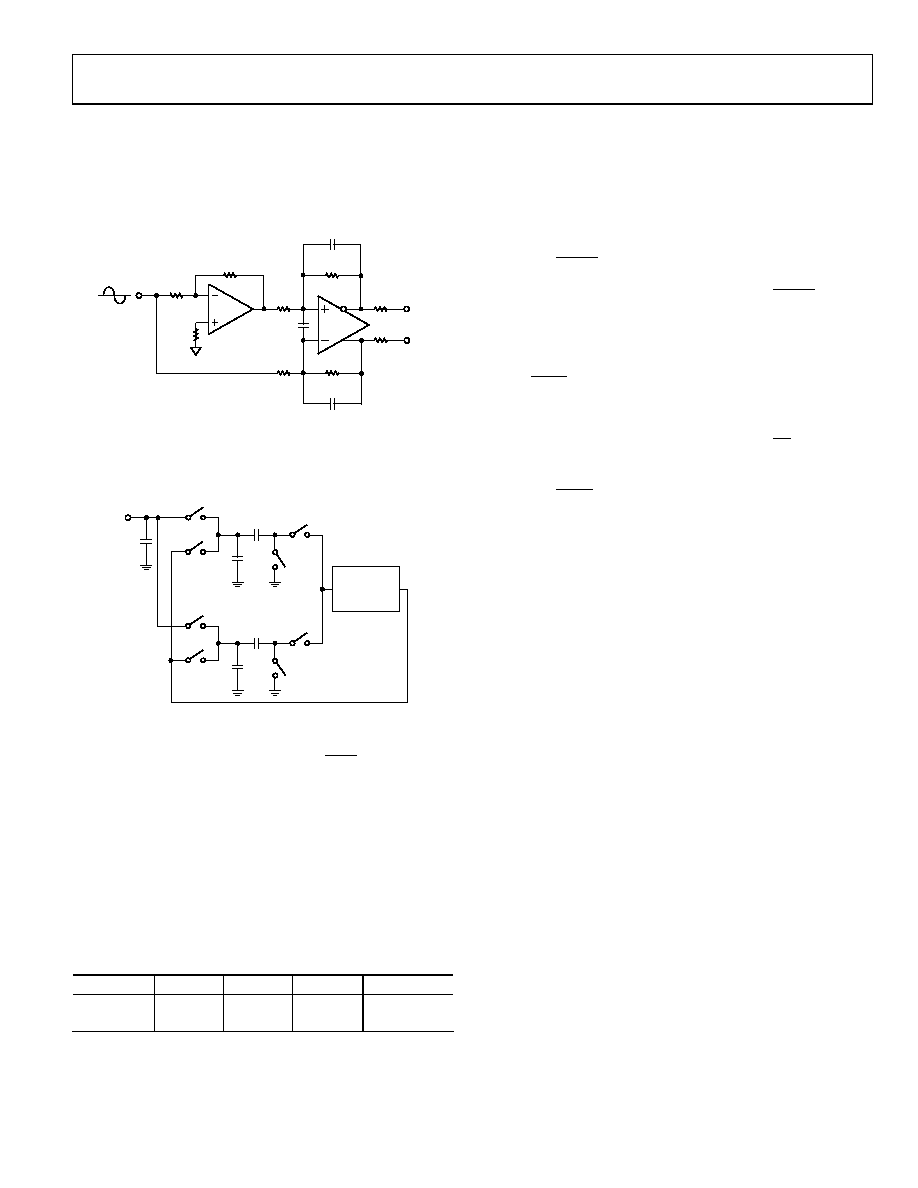
To obtain maximum performance from the AD7760, it is
advisable to drive the ADC with differential signals. Figure 53
shows how a bipolar, single-ended signal biased around ground
can drive the AD7760 with the use of an external op amp, such
as the AD8021.
A1
RIN
RFB
CFB
RIN
RM
CS
RFB
CFB
VIN–
VIN
VIN+
AD8021
2R
R
0
4
975
-04
2
Figure 53. Single-Ended-to-Differential Conversion
The AD7760 employs a double-sampling front end, as shown in
is shown. The equivalent input circuitry for VIN is the same.
CS2
CPB2
SS4
SH4
CPA
SS2
SH2
CS1
CPB1
SS3
SH3
SS1
SH1
ANALOG
MODULATOR
VIN+
04
97
5-
0
43
Figure 54. Equivalent Input Circuit
Sampling Switches SS1 and SS3 are driven by ICLK, whereas
Sampling Switches SS2 and SS4 are driven by ICLK. When ICLK is
high, the analog input voltage is connected to CS1. On the falling
edge of ICLK, the SS1 and SS3 switches open and the analog input
is sampled on CS1. Similarly, when ICLK is low, the analog input
voltage is connected to CS2. On the rising edge of ICLK, the SS2
and SS4 switches open and the analog input is sampled
on CS2.
Capacitors CPA, CPB1, and CPB2 represent parasitic capacitances
that include the junction capacitances associated with the MOS
switches.
Table 9. Equivalent Component Values
Mode
CS1 (pF)
CS2 (pF)
CPA (pF)
CPB1/2 (pF)
Normal
51
12
20
Low Power
13
12
5
USING THE AD7760
The following is the recommended sequence for powering up
and using the AD7760:
1.
Apply power.
2.
Start the clock oscillator, applying MCLK.
3.
Take RESET low for a minimum of one MCLK cycle.
4.
Wait a minimum of two MCLK cycles after RESET has
been released.
5.
Write to Control Register 2 to power up the ADC and the
differential amplifier as required. The correct clock divider
(CDIV) ratio should be programmed at this time.
6.
Write to Control Register 1 to set the output data rate.
7.
Wait a minimum of five MCLK cycles after CS has been
released.
8.
Take SYNC low for a minimum of four MCLK cycles, if
required, to synchronize multiple parts.
Data can then be read from the part using the default filter,
offset, gain, and overrange threshold values. The conversion
data read is not valid, however, until the group delay of the filter
has elapsed. Once this has occurred, the DVALID bit read with
the data LSW is set, indicating that the data is indeed valid.
The user can then download a different filter if required (see the
Downloading a User-Defined Filter section). Values for gain,
offset, and overrange threshold registers can be written or read
at this stage.
相关PDF资料 |
PDF描述 |
|---|---|
| GCM22DCMD | CONN EDGECARD 44POS .156 WW |
| REC5-4815DRW/H2/C | CONV DC/DC 5W 36-72VIN +/-15VOUT |
| ISL5861EVAL2 | EVALUATION PLATFORM ISL5861 TSSO |
| REC5-4815DRW/H2/A | CONV DC/DC 5W 36-72VIN +/-15VOUT |
| GCA18DTMN | CONN EDGECARD 36POS R/A .125 SLD |
相关代理商/技术参数 |
参数描述 |
|---|---|
| EVAL-AD7762EB | 制造商:Analog Devices 功能描述:EVALUATION CONTROL BOARD I.C. - Bulk |
| EVAL-AD7762EBZ | 制造商:Analog Devices 功能描述:EVALUATION CONTROL BOARD I.C. - Bulk |
| EVAL-AD7762EDZ | 功能描述:BOARD EVAL CONTROL AD7762 RoHS:是 类别:编程器,开发系统 >> 评估板 - 模数转换器 (ADC) 系列:- 产品培训模块:Obsolescence Mitigation Program 标准包装:1 系列:- ADC 的数量:1 位数:12 采样率(每秒):94.4k 数据接口:USB 输入范围:±VREF/2 在以下条件下的电源(标准):- 工作温度:-40°C ~ 85°C 已用 IC / 零件:MAX11645 已供物品:板,软件 |
| EVAL-AD7763EB | 制造商:Analog Devices 功能描述:EVALUATION BOARD I.C. - Bulk |
| EVAL-AD7763EBZ | 制造商:Analog Devices 功能描述:EVALUATION BOARD I.C. - Bulk |
发布紧急采购,3分钟左右您将得到回复。