参数资料
| 型号: | EVAL-ADE7759EBZ |
| 厂商: | Analog Devices Inc |
| 文件页数: | 5/36页 |
| 文件大小: | 0K |
| 描述: | BOARD EVALUATION FOR ADE7759 |
| 标准包装: | 1 |
| 主要目的: | 电源管理,电度表/功率表 |
| 已用 IC / 零件: | ADE7759 |
| 已供物品: | 板 |
| 相关产品: | ADE7759ARSZRL-ND - IC ENERGY METERING 1PHASE 20SSOP ADE7759ARSZ-ND - IC ENERGY METERING 1PHASE 20SSOP |
第1页第2页第3页第4页当前第5页第6页第7页第8页第9页第10页第11页第12页第13页第14页第15页第16页第17页第18页第19页第20页第21页第22页第23页第24页第25页第26页第27页第28页第29页第30页第31页第32页第33页第34页第35页第36页
�� ��
��
��ADE7759�
�TIMING� CHARACTERISTICS� 1,� 2�
�(AV� DD� =� DV� DD� =� 5� V� 5%,� AGND� =� DGND� =� 0� V,� On-Chip� Reference,� CLKIN� =� 3.579545� MHz�
�XTAL,� T� MIN� to� T� MAX� =� –40� C� to� +85� C,� unless� otherwise� noted.)�
�Parameter�
�A,� B� Versions�
�Unit�
�Test� Conditions/Comments�
�Write� Timing�
�t� 1�
�t� 2�
�t� 3�
�t� 4�
�t� 5�
�t� 6�
�t� 7�
�t� 8�
�Read� Timing�
�t� 9�
�t� 10�
�t� 113�
�20�
�150�
�150�
�10�
�5�
�6.4�
�4�
�100�
�4�
�4�
�30�
�ns� (min)�
�ns� (min)�
�ns� (min)�
�ns� (min)�
�ns� (min)�
�m� s� (min)�
�m� s� (min)�
�ns� (min)�
�m� s� (min)�
�m� s� (min)�
�ns� (min)�
�CS� Falling� Edge� to� First� SCLK� Falling� Edge�
�SCLK� Logic� High� Pulsewidth�
�SCLK� Logic� Low� Pulsewidth�
�Valid� Data� Setup� Time� before� Falling� Edge� of� SCLK�
�Data� Hold� Time� after� SCLK� Falling� Edge�
�Minimum� Time� between� the� End� of� Data� Byte� Transfers�
�Minimum� Time� between� Byte� Transfers� during� a� Serial� Write�
�CS� Hold� Time� after� SCLK� Falling� Edge�
�Minimum� Time� between� Read� Command� (i.e.,� a� Write� to� Communications�
�Register)� and� Data� Read�
�Minimum� Time� between� Data� Byte� Transfers� during� a� Multibyte� Read�
�Data� Access� Time� after� SCLK� Rising� Edge� following� a� Write� to� the� Communica-�
�tions� Register�
�t� 124�
�t� 134�
�100�
�10�
�100�
�10�
�ns� (max)�
�ns� (min)�
�ns� (max)�
�ns� (min)�
�Bus� Relinquish� Time� after� Falling� Edge� of� SCLK�
�Bus� Relinquish� Time� after� Rising� Edge� of� CS�
�NOTES�
�1�
�2�
�3�
�4�
�Sample� tested� during� initial� release� and� after� any� redesign� or� process� change� that� may� affect� this� parameter.� All� input� signals� are� specified� with� tr� =� tf� =� 5� ns�
�(10%� to� 90%)� and� timed� from� a� voltage� level� of� 1.6� V.�
�See� Figures� 2� and� 3� and� Serial� Interface� section� of� this� data� sheet.�
�Measured� with� the� load� circuit� in� Figure� 1� and� defined� as� the� time� required� for� the� output� to� cross� 0.8� V� or� 2.4� V.�
�Derived� from� the� measured� time� taken� by� the� data� outputs� to� change� 0.5� V� when� loaded� with� the� circuit� in� Figure� 1.� The� measured� number� is� then� extrapolated� back�
�to� remove� the� effects� of� charging� or� discharging� the� 50� pF� capacitor.� This� means� that� the� time� quoted� in� the� timing� characteristics� is� the� true� bus� relinquish� time� of�
�the� part� and� is� independent� of� the� bus� loading.�
�TO�
�200� A�
�I� OL�
�OUTPUT�
�PIN�
�C� L�
�50pF�
�1.6mA�
�I� OH�
�2.1V�
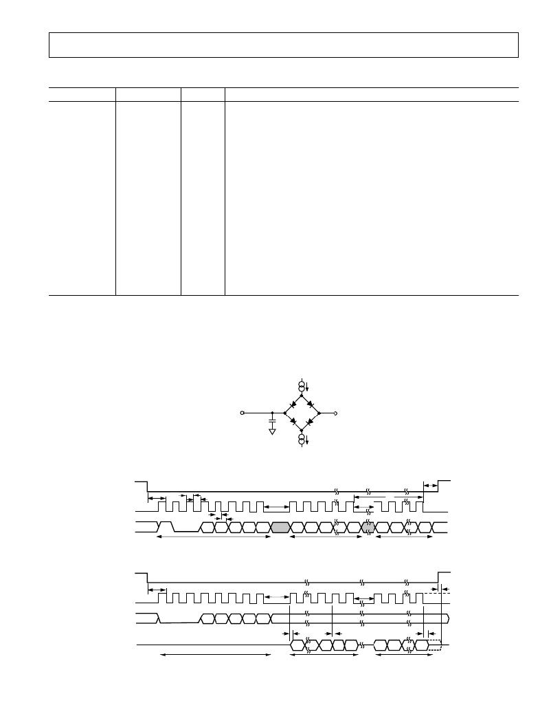
�Figure� 1.� Load� Circuit� for� Timing� Specifications�
�t� 8�
�CS�
�SCLK�
�t� 1�
�t� 2�
�t� 3�
�t� 7�
�t� 7�
�t� 6�
�t� 4�
�t� 5�
�DIN�
�1�
�0�
�0�
�A4�
�A3�
�A2�
�A1�
�A0�
�DB7�
�DB0�
�DB7�
�DB0�
�COMMAND� BYTE�
�MOST� SIGNIFICANT� BYTE�
�LEAST� SIGNIFICANT� BYTE�
�Figure� 2.� Serial� Write� Timing�
�CS�
�SCLK�
�t� 1�
�t� 9�
�t� 10�
�t� 13�
�DIN�
�0�
�0�
�0�
�A4�
�A3�
�A2�
�A1�
�A0�
�t� 11�
�t� 11�
�t� 12�
�DOUT�
�DB7�
�DB0�
�DB7�
�DB0�
�COMMAND� BYTE�
�MOST� SIGNIFICANT� BYTE�
�LEAST� SIGNIFICANT� BYTE�
�Figure� 3.� Serial� Read� Timing�
�REV.� A�
�–5� –�
�相关PDF资料 |
PDF描述 |
|---|---|
| EVAL-ADE7762EBZ | BOARD EVALUATION FOR ADE7762 |
| EVAL-ADE7763ZEB | BOARD EVALUATION FOR ADE7763 |
| EVAL-ADE7816EBZ | BOARD EVALUATION FOR ADE7816 |
| EVAL-ADE7878EBZ | BOARD EVAL FOR ADE7878 |
| EVAL-ADE7880EBZ | BOARD EVAL FOR ADE7880 |
相关代理商/技术参数 |
参数描述 |
|---|---|
| EVAL-ADE7762EBZ | 功能描述:BOARD EVALUATION FOR ADE7762 RoHS:是 类别:编程器,开发系统 >> 评估演示板和套件 系列:- 标准包装:1 系列:- 主要目的:电信,线路接口单元(LIU) 嵌入式:- 已用 IC / 零件:IDT82V2081 主要属性:T1/J1/E1 LIU 次要属性:- 已供物品:板,电源,线缆,CD 其它名称:82EBV2081 |
| EVAL-ADE7763EB | 制造商:Analog Devices 功能描述:EVALUATION BOARD DOCUMENTATION ADE7763 ENERGY METERING IC |
| EVAL-ADE7763ZEB | 功能描述:BOARD EVALUATION FOR ADE7763 RoHS:是 类别:编程器,开发系统 >> 评估演示板和套件 系列:- 标准包装:1 系列:PSoC® 主要目的:电源管理,热管理 嵌入式:- 已用 IC / 零件:- 主要属性:- 次要属性:- 已供物品:板,CD,电源 |
| EVAL-ADE7816EBZ | 功能描述:BOARD EVALUATION FOR ADE7816 RoHS:是 类别:编程器,开发系统 >> 评估演示板和套件 系列:- 标准包装:1 系列:PSoC® 主要目的:电源管理,热管理 嵌入式:- 已用 IC / 零件:- 主要属性:- 次要属性:- 已供物品:板,CD,电源 |
| EVAL-ADE7854EBZ | 制造商:Analog Devices 功能描述:EVALUATION BOARDS - Boxed Product (Development Kits) |
发布紧急采购,3分钟左右您将得到回复。