- 您现在的位置:买卖IC网 > PDF目录17112 > EVAL-ADUC834QSZ (Analog Devices Inc)KIT DEV QUICK START ADUC834 PDF资料下载
参数资料
| 型号: | EVAL-ADUC834QSZ |
| 厂商: | Analog Devices Inc |
| 文件页数: | 40/80页 |
| 文件大小: | 0K |
| 描述: | KIT DEV QUICK START ADUC834 |
| 标准包装: | 1 |
| 系列: | QuickStart™ 套件 |
| 类型: | MCU |
| 适用于相关产品: | ADuC834 |
| 所含物品: | 评估板,线缆,电源,软件和文档 |
第1页第2页第3页第4页第5页第6页第7页第8页第9页第10页第11页第12页第13页第14页第15页第16页第17页第18页第19页第20页第21页第22页第23页第24页第25页第26页第27页第28页第29页第30页第31页第32页第33页第34页第35页第36页第37页第38页第39页当前第40页第41页第42页第43页第44页第45页第46页第47页第48页第49页第50页第51页第52页第53页第54页第55页第56页第57页第58页第59页第60页第61页第62页第63页第64页第65页第66页第67页第68页第69页第70页第71页第72页第73页第74页第75页第76页第77页第78页第79页第80页
REV. A
ADuC834
–45–
SPIDAT
SPI Data Register
Function
The SPIDAT SFR is written by the user to transmit data over the SPI interface or read by user
code to read data just received by the SPI interface.
SFR Address
F7H
Power-On Default Value
00H
Bit Addressable
No
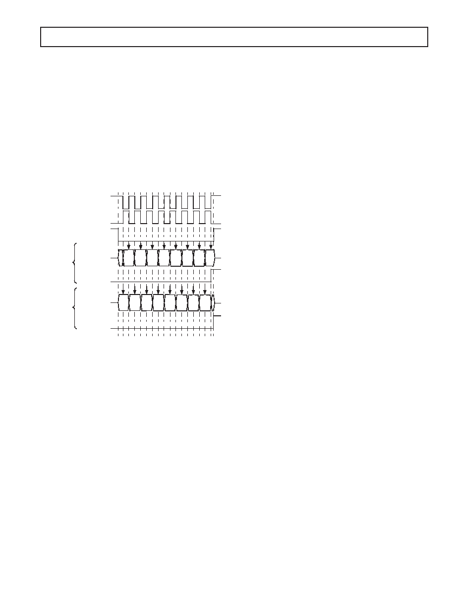
Using the SPI Interface
Depending on the configuration of the bits in the SPICON SFR
shown in Table XXI, the ADuC834 SPI interface will transmit
or receive data in a number of possible modes. Figure 34 shows
all possible ADuC834 SPI configurations and the timing rela-
tionships and synchronization between the signals involved.
Also shown in this figure is the SPI interrupt bit (ISPI) and how
it is triggered at the end of each byte-wide communication.
SCLOCK
(CPOL = 1)
SCLOCK
(CPOL = 0)
(CPHA = 1)
(CPHA = 0)
SAMPLE INPUT
ISPI FLAG
DATA OUTPUT
ISPI FLAG
SAMPLE INPUT
DATA OUTPUT
?
MSB BIT 6 BIT 5
?
BIT 4 BIT 3 BIT 2 BIT 1 LSB
MSB BIT 6 BIT 5 BIT 4 BIT 3 BIT 2 BIT 1 LSB
SS
Figure 34. SPI Timing, All Modes
SPI Interface—Master Mode
In Master Mode, the SCLOCK pin is always an output and
generates a burst of eight clocks whenever user code writes to
the SPIDAT Register. The SCLOCK bit rate is determined by
SPR0 and SPR1 in SPICON. It should also be noted that the
SS Pin is not used in Master mode. If the ADuC834 needs to
assert the
SS Pin on an external slave device, a port digital output
pin should be used.
In Master Mode, a byte transmission or reception is initiated by
a write to SPIDAT. Eight clock periods are generated via the
SCLOCK pin and the SPIDAT byte being transmitted via
MOSI. With each SCLOCK period, a data bit is also sampled
via MISO. After eight clocks, the transmitted byte will have
been completely transmitted and the input byte will be waiting
in the input shift register. The ISPI flag will be set automatically
and an interrupt will occur if enabled. The value in the shift
register will be latched into SPIDAT.
SPI Interface—Slave Mode
In Slave Mode, the SCLOCK is an input. The
SS pin must also
be driven low externally during the byte communication. Trans-
mission is also initiated by a write to SPIDAT. In Slave Mode,
a data bit is transmitted via MISO and a data bit is received via
MOSI through each input SCLOCK period. After eight clocks,
the transmitted byte will have been completely transmitted and
the input byte will be waiting in the input shift register. The ISPI
flag will be set automatically and an interrupt will occur if enabled.
The value in the shift register will be latched into SPIDAT
only when the transmission/reception of a byte has been com-
pleted. The end of transmission occurs after the eighth clock has
been received, if CPHA = 1 or when
SS returns high if CPHA = 0.
相关PDF资料 |
PDF描述 |
|---|---|
| EVAL-ADUC847QSZ | KIT DEV QUICK START FOR ADUC847 |
| GBM24DTKT | CONN EDGECARD 48POS DIP .156 SLD |
| EVAL-ADUC7026QSZ | KIT DEV FOR ADUC7026/7027 |
| GEM36DSXS | CONN EDGECARD 72POS DIP .156 SLD |
| GBM18DSAI | CONN EDGECARD 36POS R/A .156 SLD |
相关代理商/技术参数 |
参数描述 |
|---|---|
| EVAL-ADUC836QS | 制造商:Analog Devices 功能描述:MCU 8BIT 8052 CISC 62KB+4KB FLASH 3.6V 48LQFP - Bulk 制造商:Analog Devices 功能描述:KIT- ADUC836 DEV SYSTEM |
| EVAL-ADUC841QS | 制造商:AD 制造商全称:Analog Devices 功能描述:MicroConverter 12-Bit ADCs and DACs with Embedded High Speed 62-kB Flash MCU |
| EVAL-ADUC841QSP2 | 制造商:AD 制造商全称:Analog Devices 功能描述:MicroConverter 12-Bit ADCs and DACs with Embedded High Speed 62-kB Flash MCU |
| EVAL-ADUC841QSPZ | 功能描述:KIT DEV QUICK START ADUC841 RoHS:是 类别:编程器,开发系统 >> 通用嵌入式开发板和套件(MCU、DSP、FPGA、CPLD等) 系列:QuickStart™ PLUS 套件 标准包装:1 系列:PICDEM™ 类型:MCU 适用于相关产品:PIC10F206,PIC16F690,PIC16F819 所含物品:板,线缆,元件,CD,PICkit 编程器 产品目录页面:659 (CN2011-ZH PDF) |
| EVAL-ADUC841QSPZ | 制造商:Analog Devices 功能描述:Silicon Manufacturer:Analog Devices C |
发布紧急采购,3分钟左右您将得到回复。