- 您现在的位置:买卖IC网 > PDF目录375778 > FDB10AN06A0 (FAIRCHILD SEMICONDUCTOR CORP) CAP 0.1UF 50V 5% X7R SMD-1206 TR-7-PA SN100 PDF资料下载
参数资料
| 型号: | FDB10AN06A0 |
| 厂商: | FAIRCHILD SEMICONDUCTOR CORP |
| 元件分类: | JFETs |
| 英文描述: | CAP 0.1UF 50V 5% X7R SMD-1206 TR-7-PA SN100 |
| 中文描述: | 12 A, 60 V, 0.0105 ohm, N-CHANNEL, Si, POWER, MOSFET, TO-263AB |
| 封装: | TO-263AB, 3 PIN |
| 文件页数: | 2/11页 |
| 文件大小: | 265K |
| 代理商: | FDB10AN06A0 |
2002 Fairchild Semiconductor Corporation
FDB10AN06A0 / FDP10AN06A0 Rev. A
F
Package Marking and Ordering Information
Electrical Characteristics
T
C
= 25
°
C unless otherwise noted
Off Characteristics
B
VDSS
On Characteristics
V
GS(TH)
Dynamic Characteristics
C
ISS
Input Capacitance
C
OSS
Output Capacitance
C
RSS
Reverse Transfer Capacitance
Q
g(TOT)
Total Gate Charge at 10V
Q
g(TH)
Threshold Gate Charge
Q
gs
Gate to Source Gate Charge
Q
gs2
Gate Charge Threshold to Plateau
Q
gd
Gate to Drain
“
Miller
”
Charge
Switching Characteristics
(V
GS
= 10V)
t
ON
Turn-On Time
t
d(ON)
Turn-On Delay Time
t
r
Rise Time
t
d(OFF)
Turn-Off Delay Time
t
f
Fall Time
t
OFF
Turn-Off Time
Drain-Source Diode Characteristics
Notes:
1:
Starting T
= 25
°
C, L = 8.58mH, I
AS
= 10A.
2:
Pulse Width = 100s
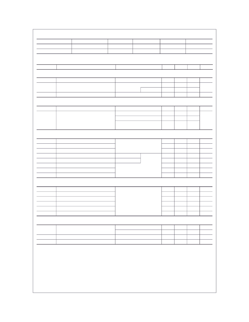
Device Marking
FDB10AN06A0
FDP10AN06A0
Device
Package
TO-263AB
TO-220AB
Reel Size
330mm
Tube
Tape Width
24mm
N/A
Quantity
800 units
50 units
FDB10AN06A0
FDP10AN06A0
Symbol
Parameter
Test Conditions
Min
Typ
Max
Units
Drain to Source Breakdown Voltage
I
D
= 250
μ
A, V
GS
= 0V
V
DS
= 50V
V
GS
= 0V
V
GS
=
±
20V
60
-
-
-
-
-
-
-
-
1
V
I
DSS
Zero Gate Voltage Drain Current
μ
A
T
C
= 150
o
C
250
±
100
I
GSS
Gate to Source Leakage Current
nA
Gate to Source Threshold Voltage
V
GS
= V
DS
, I
D
= 250
μ
A
I
D
= 75A, V
GS
= 10V
I
D
= 37A, V
GS
= 6V
I
D
= 75A, V
GS
= 10V,
T
J
= 175
o
C
2
-
-
-
4
V
r
DS(ON)
Drain to Source On Resistance
0.0095 0.0105
0.017
0.027
-
0.021
0.023
V
DS
= 25V, V
GS
= 0V,
f = 1MHz
-
-
-
1840
340
110
28
3.5
11.7
8.2
7.4
-
-
-
pF
pF
pF
nC
nC
nC
nC
nC
V
GS
= 0V to 10V
V
GS
= 0V to 2V
V
DD
= 30V
I
D
= 75A
I
g
= 1.0mA
37
4.6
-
-
-
-
-
-
-
V
DD
= 30V, I
D
= 75A
V
GS
= 10V, R
GS
= 10
-
-
-
-
-
-
-
8
206
-
-
-
-
94
ns
ns
ns
ns
ns
ns
128
27
36
-
V
SD
Source to Drain Diode Voltage
I
SD
= 75A
I
SD
= 40A
I
SD
= 75A, dI
SD
/dt = 100A/
μ
s
I
SD
= 75A, dI
SD
/dt = 100A/
μ
s
-
-
-
-
-
-
-
-
1.25
1.0
27
23
V
V
ns
nC
t
rr
Q
RR
Reverse Recovery Time
Reverse Recovered Charge
相关PDF资料 |
PDF描述 |
|---|---|
| FDP120AN15A0 | N-Channel PowerTrench MOSFET |
| FDD120AN15A | N-Channel PowerTrench MOSFET |
| FDD120AN15A0 | N-Channel PowerTrench MOSFET |
| FDP12N50 | N-Channel MOSFET 500V, 11.5A, 0.65ヘ |
| FDP13AN06A | N-Channel PowerTrench MOSFET 60V, 62A, 13.5mз |
相关代理商/技术参数 |
参数描述 |
|---|---|
| FDB10AN06A0_Q | 功能描述:MOSFET N-Channel PowerTrench RoHS:否 制造商:STMicroelectronics 晶体管极性:N-Channel 汲极/源极击穿电压:650 V 闸/源击穿电压:25 V 漏极连续电流:130 A 电阻汲极/源极 RDS(导通):0.014 Ohms 配置:Single 最大工作温度: 安装风格:Through Hole 封装 / 箱体:Max247 封装:Tube |
| FDB110N15A | 功能描述:MOSFET 150V N-Channel PowerTrench MOSFET RoHS:否 制造商:STMicroelectronics 晶体管极性:N-Channel 汲极/源极击穿电压:650 V 闸/源击穿电压:25 V 漏极连续电流:130 A 电阻汲极/源极 RDS(导通):0.014 Ohms 配置:Single 最大工作温度: 安装风格:Through Hole 封装 / 箱体:Max247 封装:Tube |
| FDB120N10 | 功能描述:MOSFET 100V N-Chan 12Mohm PowerTrench RoHS:否 制造商:STMicroelectronics 晶体管极性:N-Channel 汲极/源极击穿电压:650 V 闸/源击穿电压:25 V 漏极连续电流:130 A 电阻汲极/源极 RDS(导通):0.014 Ohms 配置:Single 最大工作温度: 安装风格:Through Hole 封装 / 箱体:Max247 封装:Tube |
| FDB12N50 | 制造商:FAIRCHILD 制造商全称:Fairchild Semiconductor 功能描述:N-Channel MOSFET 500V, 11.5A, 0.65ヘ |
| FDB12N50F | 制造商:FAIRCHILD 制造商全称:Fairchild Semiconductor 功能描述:N-Channel MOSFET, FRFET 500V, 11.5A, 0.7ヘ |
发布紧急采购,3分钟左右您将得到回复。