- 您现在的位置:买卖IC网 > Datasheet目录414 > FDB12N50TM (Fairchild Semiconductor)MOSFET N-CH 500V 11.5A D2PAK Datasheet资料下载
参数资料
| 型号: | FDB12N50TM |
| 厂商: | Fairchild Semiconductor |
| 文件页数: | 1/8页 |
| 文件大小: | 0K |
| 描述: | MOSFET N-CH 500V 11.5A D2PAK |
| 产品目录绘图: | D2PAK, TO-263AB Pkg |
| 标准包装: | 1 |
| 系列: | UniFET™ |
| FET 型: | MOSFET N 通道,金属氧化物 |
| FET 特点: | 标准 |
| 漏极至源极电压(Vdss): | 500V |
| 电流 - 连续漏极(Id) @ 25° C: | 11.5A |
| 开态Rds(最大)@ Id, Vgs @ 25° C: | 650 毫欧 @ 6A,10V |
| Id 时的 Vgs(th)(最大): | 5V @ 250µA |
| 闸电荷(Qg) @ Vgs: | 30nC @ 10V |
| 输入电容 (Ciss) @ Vds: | 1315pF @ 25V |
| 功率 - 最大: | 165W |
| 安装类型: | 表面贴装 |
| 封装/外壳: | TO-263-3,D²Pak(2 引线+接片),TO-263AB |
| 供应商设备封装: | D²PAK |
| 包装: | 标准包装 |
| 其它名称: | FDB12N50TMDKR |
�� �
�
�November� 2013�
�FDB12N50TM�
�N-Channel� UniFET� TM� MOSFET�
�500� V,� 11.5� A,� 650� m� ?�
�Features�
�?� R� DS(on)� =� 550� m� ?� (Typ.)� @� V� GS� =� 10� V,� I� D� =� 6� A�
�?� Low� Gate� Charge� (Typ.� 22� nC)�
�?� Low� C� rss� (Typ.� 12� pF)�
�?� 100%� Avalanche� Tested�
�?� RoHS� Compliant�
�Applications�
�Description�
�UniFET� TM� MOSFET� is� Fairchild� Semiconductor� ’s� high� voltage�
�MOSFET� family� based� on� planar� stripe� and� DMOS� technology.�
�This� MOSFET� is� tailored� to� reduce� on-state� resistance,� and� to�
�provide� better� switching� performance� and� higher� avalanche�
�energy� strength.� This� device� family� is� suitable� for� switching�
�power� converter� applications� such� as� power� factor� correction�
�(PFC),� flat� panel� display� (FPD)� TV� power,� ATX� and� electronic�
�lamp� ballasts.�
�?� Lighting�
�?� Uninterruptible� Power� Supply�
�?� AC-DC� Power� Supply�
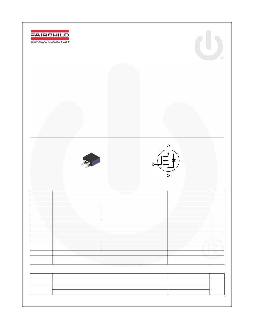
�D�
�D�
�G�
�S�
�D� 2� -PAK�
�G�
�S�
�MOSFET� Maximum� Ratings� T� C� =� 25� o� C� unless� otherwise� noted.�
�Symbol�
�V� DSS�
�Drain� to� Source� Voltage�
�Parameter�
�FDB12N50TM�
�500�
�Unit�
�V�
�V� GSS�
�I� D�
�Gate� to� Source� Voltage�
�Drain� Current�
�-� Continuous� (T� C� =� 25� o� C)�
�-� Continuous� (T� C� =� 100� o� C)�
�±30�
�11.5�
�6.9�
�V�
�A�
�I� DM�
�Drain� Current�
�-� Pulsed�
�(Note� 1)�
�46�
�A�
�E� AS�
�I� AR�
�E� AR�
�dv/dt�
�P� D�
�Single� Pulsed� Avalanche� Energy�
�Avalanche� Current�
�Repetitive� Avalanche� Energy�
�Peak� Diode� Recovery� dv/dt�
�Power� Dissipation�
�(T� C� =� 25� o� C)�
�-� Derate� above� 25� o� C�
�(Note� 2)�
�(Note� 1)�
�(Note� 1)�
�(Note� 3)�
�456�
�11.5�
�16.7�
�4.5�
�165�
�1.33�
�mJ�
�A�
�mJ�
�V/ns�
�W�
�W/� o� C�
�T� J� ,� T� STG�
�T� L�
�Operating� and� Storage� Temperature� Range�
�Maximum� Lead� Temperature� for� Soldering� Purpose,�
�1/8”� from� Case� for� 5� Seconds�
�-55� to� +150�
�300�
�o�
�o�
�C�
�C�
�Thermal� Characteristics�
�Symbol�
�R� ?� JC�
�Parameter�
�Thermal� Resistance,� Junction� to� Case,� Max�
�FDB12N50TM�
�0.75�
�Unit�
�R� ?� JA�
�Thermal� Resistance,� Junction� to� Ambient� (minimum� pad� of� 2� oz� copper),� Max.�
�Thermal� Resistance,� Junction� to� Ambient� (1� in� 2� pad� of� 2� oz� copper),� Max.�
�62.5�
�40�
�o�
�C/W�
�?2007� Fairchild� Semiconductor� Corporation�
�FDB12N50TM� Rev.� C1�
�1�
�www.fairchildsemi.com�
�相关PDF资料 |
PDF描述 |
|---|---|
| FDB12N50UTM_WS | MOSFET N-CH 500V 10A D2PAK |
| FDB14AN06LA0_F085 | MOSFET N-CH 60V 67A D2PAK |
| FDB14N30TM | MOSFET N-CH 300V 14A D2PAK |
| FDB150N10 | MOSFET N-CH 100V 57A D2PAK |
| FDB15N50 | MOSFET N-CH 500V 15A TO-263AB |
相关代理商/技术参数 |
参数描述 |
|---|---|
| FDB12N50U | 制造商:FAIRCHILD 制造商全称:Fairchild Semiconductor 功能描述:N-Channel MOSFET, FRFET 500V, 10A, 0.8ヘ |
| FDB12N50U_12 | 制造商:FAIRCHILD 制造商全称:Fairchild Semiconductor 功能描述:N-Channel MOSFET, FRFET 500V, 10A, 0.8?? |
| FDB12N50UTM | 制造商:Rochester Electronics LLC 功能描述: 制造商:Fairchild Semiconductor Corporation 功能描述: |
| FDB12N50UTM_12 | 制造商:FAIRCHILD 制造商全称:Fairchild Semiconductor 功能描述:N-Channel MOSFET, FRFET 500V, 10A, 0.8?? |
| FDB12N50UTM_WS | 功能描述:MOSFET 500V 10A 0.8Ohm N-Channel RoHS:否 制造商:STMicroelectronics 晶体管极性:N-Channel 汲极/源极击穿电压:650 V 闸/源击穿电压:25 V 漏极连续电流:130 A 电阻汲极/源极 RDS(导通):0.014 Ohms 配置:Single 最大工作温度: 安装风格:Through Hole 封装 / 箱体:Max247 封装:Tube |
发布紧急采购,3分钟左右您将得到回复。