- 您现在的位置:买卖IC网 > Datasheet目录414 > FDB14AN06LA0_F085 (Fairchild Semiconductor)MOSFET N-CH 60V 67A D2PAK Datasheet资料下载
参数资料
| 型号: | FDB14AN06LA0_F085 |
| 厂商: | Fairchild Semiconductor |
| 文件页数: | 1/11页 |
| 文件大小: | 0K |
| 描述: | MOSFET N-CH 60V 67A D2PAK |
| 标准包装: | 800 |
| 系列: | PowerTrench® |
| FET 型: | MOSFET N 通道,金属氧化物 |
| FET 特点: | 逻辑电平门 |
| 漏极至源极电压(Vdss): | 60V |
| 电流 - 连续漏极(Id) @ 25° C: | 67A |
| 开态Rds(最大)@ Id, Vgs @ 25° C: | 11.6 毫欧 @ 67A,10V |
| Id 时的 Vgs(th)(最大): | 3V @ 250µA |
| 闸电荷(Qg) @ Vgs: | 31nC @ 5V |
| 输入电容 (Ciss) @ Vds: | 2900pF @ 25V |
| 功率 - 最大: | 125W |
| 安装类型: | 表面贴装 |
| 封装/外壳: | TO-263-3,D²Pak(2 引线+接片),TO-263AB |
| 供应商设备封装: | TO-263 |
| 包装: | 带卷 (TR) |
�� �
�
�December� 2010�
�FDB14AN06LA0_F085�
�N-Channel� PowerTrench� ?� MOSFET�
�60V,� 60A,� 14.6m� ?�
�Features�
�?� r� DS(ON)� =� 12.8m� ?� (Typ.),� V� GS� =� 5V,� I� D� =� 60A�
�?� Q� g� (tot)� =� 24nC� (Typ.),� V� GS� =� 5V�
�?� Low� Miller� Charge�
�?� Low� Q� RR� Body� Diode�
�?� UIS� Capability� (Single� Pulse� and� Repetitive� Pulse)�
�? Qualified to AEC Q101�
�?� RoHS� Compliant�
�Applications�
�?� Motor� /� Body� Load� Control�
�?� ABS� Systems�
�?� Powertrain� Management�
�?� Injection� Systems�
�?� DC-DC� converters� and� Off-line� UPS�
�? Distributed Power Architectures and VRMs�
�?� Primary� Switch� for� 12V� and� 24V� systems�
�Formerly� developmental� type� 83557�
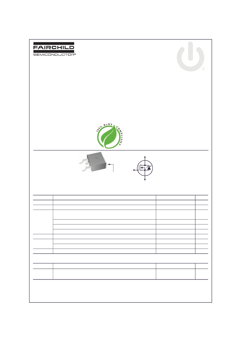
�D�
�GATE�
�G�
�SOURCE�
�DRAIN�
�TO-263AB�
�(FLANGE)�
�S�
�FDB� SERIES�
�MOSFET� Maximum� Ratings� T� C� =� 25°C� unless� otherwise� noted�
�Symbol�
�V� DSS�
�V� GS�
�Drain� to� Source� Voltage�
�Gate� to� Source� Voltage�
�Parameter�
�Ratings�
�60�
�±� 20�
�Units�
�V�
�V�
�Drain� Current�
�Continuous� (T� C� =� 25� o� C,� V� GS� =� 10V)�
�67�
�A�
�Continuous� (T� C� =� 25� C,� V� GS� =� 5V)�
�C�
�I� D�
�E� AS�
�P� D�
�T� J� ,� T� STG�
�o�
�Continuous� (T� A� =� 25� o� C,� V� GS� =� 5V,� R� θ� JA� =� 43� o� C/W)�
�Pulsed�
�Single� Pulse� Avalanche� Energy� (Note� 1)�
�Power� dissipation�
�Derate� above� 25� o� C�
�Operating� and� Storage� Temperature�
�60�
�10�
�Figure� 4�
�46�
�125�
�0.83�
�-55� to� 175�
�A�
�A�
�A�
�mJ�
�W�
�W/� o� C�
�o�
�Thermal� Characteristics�
�R� θ� JC�
�Maximum� Thermal� Resistance� Junction� to� Case� TO-263�
�1.2�
�o� C/W�
�R� θ� JA�
�Maximum� Thermal� Resistance� Junction� to� Ambient� TO-263,� 1in� 2�
�copper� pad� area�
�43�
�o�
�C/W�
�This� product� has� been� designed� to� meet� the� extreme� test� conditions� and� environment� demanded� by� the� automotive� industry.� For� a�
�copy� of� the� requirements,� see� AEC� Q101� at:� http://www.aecouncil.com/�
�Reliability� data� can� be� found� at:� http://www.fairchildsemi.com/products/discrete/reliability/index.html.�
�All� Fairchild� Semiconductor� products� are� manufactured,� assembled� and� tested� under� ISO9000� and� QS9000� quality� systems�
�certification.�
�?2010� Fairchild� Semiconductor� Corporation�
�FDB14AN06LA0_F085� Rev.� C�
�相关PDF资料 |
PDF描述 |
|---|---|
| FDB14N30TM | MOSFET N-CH 300V 14A D2PAK |
| FDB150N10 | MOSFET N-CH 100V 57A D2PAK |
| FDB15N50 | MOSFET N-CH 500V 15A TO-263AB |
| FDB2532_F085 | MOSFET N-CH 150V 79A D2PAK |
| FDB2614 | MOSFET N-CH 200V 62A D2PAK |
相关代理商/技术参数 |
参数描述 |
|---|---|
| FDB14N30 | 制造商:FAIRCHILD 制造商全称:Fairchild Semiconductor 功能描述:300V N-Channel MOSFET |
| FDB14N30TM | 功能描述:MOSFET 300V N-Ch MOSFET RoHS:否 制造商:STMicroelectronics 晶体管极性:N-Channel 汲极/源极击穿电压:650 V 闸/源击穿电压:25 V 漏极连续电流:130 A 电阻汲极/源极 RDS(导通):0.014 Ohms 配置:Single 最大工作温度: 安装风格:Through Hole 封装 / 箱体:Max247 封装:Tube |
| FDB150N10 | 功能描述:MOSFET 100V N-Channel PowerTrench RoHS:否 制造商:STMicroelectronics 晶体管极性:N-Channel 汲极/源极击穿电压:650 V 闸/源击穿电压:25 V 漏极连续电流:130 A 电阻汲极/源极 RDS(导通):0.014 Ohms 配置:Single 最大工作温度: 安装风格:Through Hole 封装 / 箱体:Max247 封装:Tube |
| FDB15N50 | 功能描述:MOSFET 15A 500V 0.38 Ohm N-Ch SMPS Pwr RoHS:否 制造商:STMicroelectronics 晶体管极性:N-Channel 汲极/源极击穿电压:650 V 闸/源击穿电压:25 V 漏极连续电流:130 A 电阻汲极/源极 RDS(导通):0.014 Ohms 配置:Single 最大工作温度: 安装风格:Through Hole 封装 / 箱体:Max247 封装:Tube |
| FDB15N50 | 制造商:Fairchild Semiconductor Corporation 功能描述:N CHANNEL MOSFET 500V 15A TO-263 |
发布紧急采购,3分钟左右您将得到回复。