- 您现在的位置:买卖IC网 > Datasheet目录424 > FDP8860 (Fairchild Semiconductor)MOSFET N-CH 30V 80A TO-220AB Datasheet资料下载
参数资料
| 型号: | FDP8860 |
| 厂商: | Fairchild Semiconductor |
| 文件页数: | 2/6页 |
| 文件大小: | 0K |
| 描述: | MOSFET N-CH 30V 80A TO-220AB |
| 产品目录绘图: | MOSFET TO-220AB |
| 标准包装: | 50 |
| 系列: | PowerTrench® |
| FET 型: | MOSFET N 通道,金属氧化物 |
| FET 特点: | 逻辑电平门 |
| 漏极至源极电压(Vdss): | 30V |
| 电流 - 连续漏极(Id) @ 25° C: | 80A |
| 开态Rds(最大)@ Id, Vgs @ 25° C: | 2.5 毫欧 @ 80A,10V |
| Id 时的 Vgs(th)(最大): | 2.5V @ 250µA |
| 闸电荷(Qg) @ Vgs: | 222nC @ 10V |
| 输入电容 (Ciss) @ Vds: | 12240pF @ 15V |
| 功率 - 最大: | 254W |
| 安装类型: | 通孔 |
| 封装/外壳: | TO-220-3 |
| 供应商设备封装: | TO-220AB |
| 包装: | 管件 |
| 产品目录页面: | 1605 (CN2011-ZH PDF) |
�� �
�
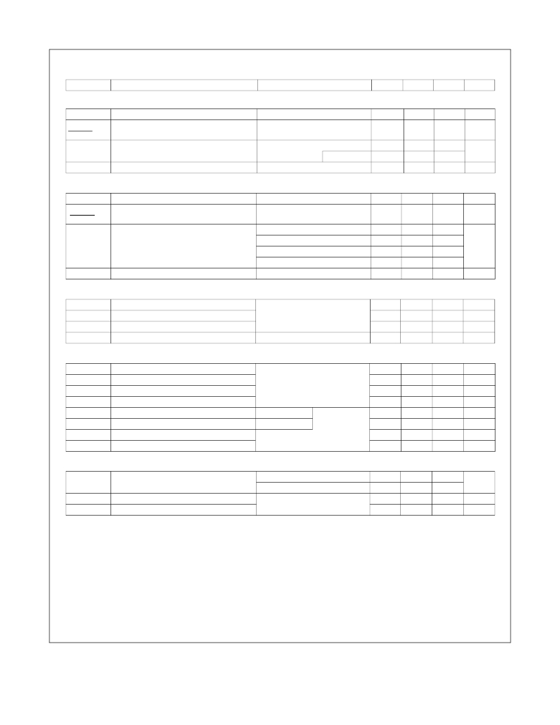
�Electrical� Characteristics� T� J� =� 25°C� unless� otherwise� noted�
�Symbol�
�Parameter�
�Test� Conditions�
�Min�
�Typ�
�Max�
�Units�
�Off� Characteristics�
�BV� DSS�
�?� BV� DS� S�
�?� T� J�
�Drain� to� Source� Breakdown� Voltage�
�Breakdown� Voltage� Temperature�
�Coefficient�
�I� D� =� 1mA,� V� GS� =� 0V�
�I� D� =� 1mA,� referenced� to� 25°C�
�30�
�22�
�V�
�mV/°� C�
�I� DSS�
�I� GSS�
�Zero� Gate� Voltage� Drain� Current�
�Gate� to� Source� Leakage� Current�
�V� DS� =� 24V,�
�V� GS� =� 0V�
�V� GS� =� ±20V�
�T� J� =� 150°C�
�1�
�250�
�±100�
�μ� A�
�nA�
�On� Characteristics�
�V� GS(th)�
�?� V� GS(th� )�
�?� T� J�
�Gate� to� Source� Threshold� Voltage�
�Gate� to� Source� Threshold� Voltage�
�Temperature� Coefficient�
�V� GS� =� V� DS� ,� I� D� =� 250� μ� A�
�I� D� =� 250� μ� A,� referenced� to� 25°C�
�1�
�1.6�
�-9.6�
�2.5�
�V�
�mV/°C�
�V� GS� =� 10V,� I� D� =� 80A�
�1.9�
�2.5�
�r� DS(on)�
�Drain� to� Source� On� Resistance�
�V� GS� =� 5V,� I� D� =� 80A�
�V� GS� =� 4.5V,� I� D� =� 80A�
�2.0�
�2.1�
�2.8�
�2.9�
�m� ?�
�V� GS� =� 10V,� I� D� =� 80A,� T� J� =� 150°C�
�2.9�
�3.8�
�g� FS�
�Forward� Transconductance�
�V� DS� =� 10V,� I� D� =� 80A�
�3.4�
�S�
�Dynamic� Characteristics�
�C� iss�
�C� oss�
�C� rss�
�R� g�
�Input� Capacitance�
�Output� Capacitance�
�Reverse� Transfer� Capacitance�
�Gate� Resistance�
�V� DS� =� 15V,� V� GS� =� 0V,�
�f� =� 1MHz�
�f� =� 1MHz�
�9200�
�1700�
�1060�
�1.7�
�12240�
�2260�
�1590�
�pF�
�pF�
�pF�
�?�
�Switching� Characteristics�
�t� d(on)�
�t� r�
�t� d(off)�
�t� f�
�Turn-On� Delay� Time�
�Rise� Time�
�Turn-Off� Delay� Time�
�Fall� Time�
�V� DD� =� 15V,� I� D� =� 80A�
�V� GS� =� 5V,� R� GEN� =� 3� ?�
�35�
�135�
�64�
�59�
�56�
�216�
�103�
�95�
�ns�
�ns�
�ns�
�ns�
�Q� g(TOT)�
�Q� g(5)�
�Q� gs�
�Total� Gate� Charge� at� 10V�
�Total� Gate� Charge� at� 5V�
�Gate� to� Source� Gate� Charge�
�V� GS� =� 0V� to� 10V�
�V� GS� =� 0V� to� 5V�
�V� DD� =� 15V�
�I� D� =� 80A�
�158�
�81�
�27�
�222�
�114�
�nC�
�nC�
�nC�
�Q� gd�
�Gate� to� Drain� “Miller”� Charge�
�33�
�nC�
�Drain-Source� Diode� Characteristics�
�V� SD�
�t� rr�
�Q� rr�
�Source� to� Drain� Diode� Forward� Voltage�
�Reverse� Recovery� Time�
�Reverse� Recovery� Charge�
�V� GS� =� 0V,� I� S� =� 80A�
�V� GS� =� 0V,� I� S� =� 40A�
�I� F� =� 80A,� di/dt� =� 100A/� μ� s�
�0.88�
�0.81�
�60�
�74�
�1.25�
�1.2�
�90�
�111�
�V�
�ns�
�nC�
�Notes:�
�1:� Pulse� Test:� Pulse� Width� <� 80� μ� s,� Duty� cycle� <� 0.5%.�
�2:� Starting� T� J� =25� o� C,� L=� 0.3mH,� I� AS� =� 67A,V� DD� =� 27V,� V� GS� =� 10V.�
�FDP8860� Rev.B�
�2�
�www.fairchildsemi.com�
�相关PDF资料 |
PDF描述 |
|---|---|
| FDP8870_F085 | MOSFET N-CH 30V 156A TO-220 |
| FDP8874 | MOSFET N-CH 30V 114A TO-220AB |
| FDP8876 | MOSFET N-CH 30V 70A TO-220 |
| FDP8880 | MOSFET N-CH 30V 54A TO-220AB |
| FDP8896 | MOSFET N-CH 30V 92A TO-220AB |
相关代理商/技术参数 |
参数描述 |
|---|---|
| FDP8870 | 功能描述:MOSFET 30V N-Channel PowerTrench RoHS:否 制造商:STMicroelectronics 晶体管极性:N-Channel 汲极/源极击穿电压:650 V 闸/源击穿电压:25 V 漏极连续电流:130 A 电阻汲极/源极 RDS(导通):0.014 Ohms 配置:Single 最大工作温度: 安装风格:Through Hole 封装 / 箱体:Max247 封装:Tube |
| FDP8870_08 | 制造商:FAIRCHILD 制造商全称:Fairchild Semiconductor 功能描述:N-Channel PowerTrench㈢ MOSFET |
| FDP8870_10 | 制造商:FAIRCHILD 制造商全称:Fairchild Semiconductor 功能描述:N-Channel PowerTrench?? MOSFET 30V, 156A, 4.1mW |
| FDP8870_F085 | 功能描述:MOSFET 30V/156A/4.1Mohm/NCH POWERTRENCH RoHS:否 制造商:STMicroelectronics 晶体管极性:N-Channel 汲极/源极击穿电压:650 V 闸/源击穿电压:25 V 漏极连续电流:130 A 电阻汲极/源极 RDS(导通):0.014 Ohms 配置:Single 最大工作温度: 安装风格:Through Hole 封装 / 箱体:Max247 封装:Tube |
| FDP8874 | 功能描述:MOSFET 30V 114A 5.3 OHM N-CH RoHS:否 制造商:STMicroelectronics 晶体管极性:N-Channel 汲极/源极击穿电压:650 V 闸/源击穿电压:25 V 漏极连续电流:130 A 电阻汲极/源极 RDS(导通):0.014 Ohms 配置:Single 最大工作温度: 安装风格:Through Hole 封装 / 箱体:Max247 封装:Tube |
发布紧急采购,3分钟左右您将得到回复。