- 您现在的位置:买卖IC网 > PDF目录11800 > FT245RQ-REEL (FTDI, Future Technology Devices International Ltd)IC USB TO PARALLEL FIFO 32-QFN PDF资料下载
参数资料
| 型号: | FT245RQ-REEL |
| 厂商: | FTDI, Future Technology Devices International Ltd |
| 文件页数: | 3/37页 |
| 文件大小: | 0K |
| 描述: | IC USB TO PARALLEL FIFO 32-QFN |
| 产品培训模块: | USB Introduction |
| 标准包装: | 1 |
| 应用: | USB 至 FIFO 控制器 |
| 接口: | USB,FIFO,(同步/异步) |
| 电源电压: | 1.8 V ~ 5.25 V |
| 封装/外壳: | 32-VFQFN 裸露焊盘 |
| 供应商设备封装: | 32-QFN 裸露焊盘(5x5) |
| 包装: | 标准包装 |
| 安装类型: | 表面贴装 |
| 产品目录页面: | 634 (CN2011-ZH PDF) |
| 配用: | 768-1020-ND - MOD USB PARALLEL FIFO DEV FT245R |
| 其它名称: | 768-1012-6 |
第1页第2页当前第3页第4页第5页第6页第7页第8页第9页第10页第11页第12页第13页第14页第15页第16页第17页第18页第19页第20页第21页第22页第23页第24页第25页第26页第27页第28页第29页第30页第31页第32页第33页第34页第35页第36页第37页
Copyright 2010 Future Technology Devices International Limited
11
Document No.: FT_000052
FT245R USB FIFO IC Datasheet Version 2.12
Clearance No.: FTDI# 39
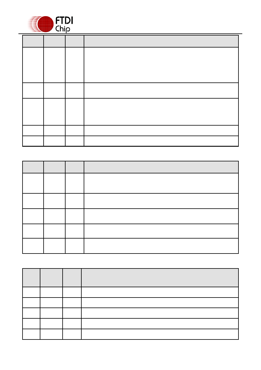
Pin No.
Name
Type
Description
1
VCCIO
PWR
+1.8V to +5.25V supply for the FIFO Interface group pins (2, 3, 6,7,8,9,10 11, 21,
22, 30,31,32). In USB bus powered designs connect this pin to 3V3OUT to drive out
at +3.3V levels, or connect to VCC to drive out at +5V CMOS level. This pin can also
be supplied with an external +1.8V to +2.8V supply in order to drive out at lower
levels. It should be noted that in this case this supply should originate from the
same source as the supply to VCC. This means that in bus powered designs a
regulator which is supplied by the +5V on the USB bus should be used.
4, 17,
20
GND
PWR
Device ground supply pins.
16
3V3OUT
Output
+3.3V output from integrated LDO regulator. This pin should be decoupled to
ground using a 100nF capacitor. The purpose of this output is to provide the
internal +3.3V supply to the USB transceiver cell and the internal 1.5kΩ pull up
resistor on USBDP. Up to 50mA can be drawn from this pin to power external logic if
required. This pin can also be used to supply the VCCIO pin.
19
VCC
PWR
+3.3V to +5.25V supply to the device core. (see Note 1).
24
AGND
PWR
Device analogue ground supply for internal clock multiplier.
Table 3.6 Power and Ground Group
Pin No.
Name
Type
Description
5, 12,
13, 23,
25, 29
NC
No internal connection. Do not connect.
18
RESET#
Input
Active low reset. Can be used by an external device to reset the FT245R. If
not required can be left unconnected, or pulled up to VCC.
26
TEST
Input
Puts the device into IC test mode. Must be tied to GND for normal
operation, otherwise the device will appear to fail.
27
OSCI
Input
Input 12MHz Oscillator Cell. Optional – Can be left unconnected for normal
operation. (see Note 2).
28
OSCO
Output
Output from 12MHZ Oscillator Cell. Optional – Can be left unconnected for
normal operation if internal Oscillator is used. (see Note 2).
Table 3.7 Miscellaneous Signal Group
Pin
No.
Name
Type
Description
30
D0
I/O
FIFO Data Bus Bit 0
31
D4
I/O
FIFO Data Bus Bit 4
32
D2
I/O
FIFO Data Bus Bit 2
2
D1
I/O
FIFO Data Bus Bit 1
3
D7
I/O
FIFO Data Bus Bit 7
相关PDF资料 |
PDF描述 |
|---|---|
| V48A12E500BG2 | CONVERTER MOD DC/DC 12V 500W |
| V48A12E500BF3 | CONVERTER MOD DC/DC 12V 500W |
| V48A12E500BF2 | CONVERTER MOD DC/DC 12V 500W |
| V48A12E500BF | CONVERTER MOD DC/DC 12V 500W |
| V48A12E500BL2 | CONVERTER MOD DC/DC 12V 500W |
相关代理商/技术参数 |
参数描述 |
|---|---|
| FT245RQ-TRAY | 制造商:Future Technology Devices International (FTDI Chip) 功能描述:Single Chip USB Tray |
| FT24B3 031175 | 制造商:Comair Rotron 功能描述:FAN 120X120X25MM 24VDC |
| FT24B3-E2 | 制造商:Comair Rotron 功能描述:FAN FLIGHT II 120X120X25MM 24V |
| FT24B3-E2 | 制造商:Comair Rotron 功能描述:FAN FLIGHT II 120X120X25 24V |
| FT24C02A | 制造商:未知厂家 制造商全称:未知厂家 功能描述:Two-Wire Serial EEPROM |
发布紧急采购,3分钟左右您将得到回复。