- 您现在的位置:买卖IC网 > PDF目录223866 > GS8342QT10BGD-300T (GSI TECHNOLOGY) 4M X 9 QDR SRAM, 0.45 ns, PBGA165 PDF资料下载
参数资料
| 型号: | GS8342QT10BGD-300T |
| 厂商: | GSI TECHNOLOGY |
| 元件分类: | SRAM |
| 英文描述: | 4M X 9 QDR SRAM, 0.45 ns, PBGA165 |
| 封装: | 13 X 15 MM, 1 MM PITCH, FPBGA-165 |
| 文件页数: | 14/30页 |
| 文件大小: | 306K |
| 代理商: | GS8342QT10BGD-300T |
第1页第2页第3页第4页第5页第6页第7页第8页第9页第10页第11页第12页第13页当前第14页第15页第16页第17页第18页第19页第20页第21页第22页第23页第24页第25页第26页第27页第28页第29页第30页
Preliminary
GS8342QT07/10/19/37BD-357/333/300/250/200
Specifications cited are subject to change without notice. For latest documentation see http://www.gsitechnology.com.
Rev: 1.00 5/2011
21/30
2011, GSI Technology
JTAG Port Operation
Overview
The JTAG Port on this RAM operates in a manner that is compliant with IEEE Standard 1149.1-1990, a serial boundary scan
interface standard (commonly referred to as JTAG). The JTAG Port input interface levels scale with VDD. The JTAG output
drivers are powered by VDD.
Disabling the JTAG Port
It is possible to use this device without utilizing the JTAG port. The port is reset at power-up and will remain inactive unless
clocked. TCK, TDI, and TMS are designed with internal pull-up circuits.To assure normal operation of the RAM with the JTAG
Port unused, TCK, TDI, and TMS may be left floating or tied to either VDD or VSS. TDO should be left unconnected.
JTAG Port Registers
Overview
The various JTAG registers, refered to as Test Access Port or TAP Registers, are selected (one at a time) via the sequences of 1s
and 0s applied to TMS as TCK is strobed. Each of the TAP Registers is a serial shift register that captures serial input data on the
rising edge of TCK and pushes serial data out on the next falling edge of TCK. When a register is selected, it is placed between the
TDI and TDO pins.
Instruction Register
The Instruction Register holds the instructions that are executed by the TAP controller when it is moved into the Run, Test/Idle, or
the various data register states. Instructions are 3 bits long. The Instruction Register can be loaded when it is placed between the
TDI and TDO pins. The Instruction Register is automatically preloaded with the IDCODE instruction at power-up or whenever the
controller is placed in Test-Logic-Reset state.
Bypass Register
The Bypass Register is a single bit register that can be placed between TDI and TDO. It allows serial test data to be passed through
the RAM’s JTAG Port to another device in the scan chain with as little delay as possible.
Boundary Scan Register
The Boundary Scan Register is a collection of flip flops that can be preset by the logic level found on the RAM’s input or I/O pins.
The flip flops are then daisy chained together so the levels found can be shifted serially out of the JTAG Port’s TDO pin. The
Boundary Scan Register also includes a number of place holder flip flops (always set to a logic 1). The relationship between the
device pins and the bits in the Boundary Scan Register is described in the Scan Order Table following. The Boundary Scan
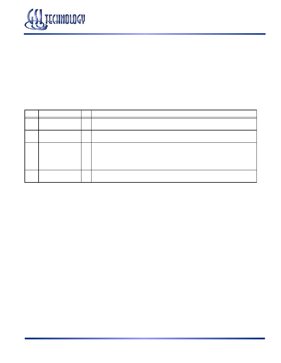
JTAG Pin Descriptions
Pin
Pin Name
I/O
Description
TCK
Test Clock
In
Clocks all TAP events. All inputs are captured on the rising edge of TCK and all outputs propagate from the
falling edge of TCK.
TMS
Test Mode Select
In
The TMS input is sampled on the rising edge of TCK. This is the command input for the TAP controller state
machine. An undriven TMS input will produce the same result as a logic one input level.
TDI
Test Data In
In
The TDI input is sampled on the rising edge of TCK. This is the input side of the serial registers placed
between TDI and TDO. The register placed between TDI and TDO is determined by the state of the TAP
Controller state machine and the instruction that is currently loaded in the TAP Instruction Register (refer to
the TAP Controller State Diagram). An undriven TDI pin will produce the same result as a logic one input
level.
TDO
Test Data Out
Out
Output that is active depending on the state of the TAP state machine. Output changes in response to the
falling edge of TCK. This is the output side of the serial registers placed between TDI and TDO.
Note:
This device does not have a TRST (TAP Reset) pin. TRST is optional in IEEE 1149.1. The Test-Logic-Reset state is entered while TMS is
held high for five rising edges of TCK. The TAP Controller is also reset automaticly at power-up.
相关PDF资料 |
PDF描述 |
|---|---|
| GS8342TT06BGD-500T | 4M X 8 DDR SRAM, 0.45 ns, PBGA165 |
| GS841Z36CGT-166IT | 128K X 36 ZBT SRAM, 7 ns, PQFP100 |
| GS842Z18CB-250T | 256K X 18 ZBT SRAM, 5.5 ns, PBGA119 |
| GS8641ZV18GE-200 | 4M X 18 ZBT SRAM, 7.5 ns, PBGA165 |
| GS8644Z18GE-225T | 4M X 18 ZBT SRAM, 6.5 ns, PBGA165 |
相关代理商/技术参数 |
参数描述 |
|---|---|
| GS8342R08AE-167 | 制造商:GSI Technology 功能描述:SRAM SYNC SGL 1.8V 36MBIT 4MX8 0.5NS 165FPBGA - Trays |
| GS8342R08AE-167I | 制造商:GSI Technology 功能描述:SRAM SYNC SGL 1.8V 36MBIT 4MX8 0.5NS 165FPBGA - Trays |
| GS8342R08AE-200 | 制造商:GSI Technology 功能描述:SRAM SYNC SGL 1.8V 36MBIT 4MX8 0.45NS 165FPBGA - Trays |
| GS8342R08AE-200I | 制造商:GSI Technology 功能描述:SRAM SYNC SGL 1.8V 36MBIT 4MX8 0.45NS 165FPBGA - Trays |
| GS8342R08AE-250 | 制造商:GSI Technology 功能描述:SRAM SYNC SGL 1.8V 36MBIT 4MX8 0.45NS 165FPBGA - Trays |
发布紧急采购,3分钟左右您将得到回复。