- 您现在的位置:买卖IC网 > PDF目录174446 > HGT1S7N60B3S9A (FAIRCHILD SEMICONDUCTOR CORP) 14 A, 600 V, N-CHANNEL IGBT, TO-263AB PDF资料下载
参数资料
| 型号: | HGT1S7N60B3S9A |
| 厂商: | FAIRCHILD SEMICONDUCTOR CORP |
| 元件分类: | IGBT 晶体管 |
| 英文描述: | 14 A, 600 V, N-CHANNEL IGBT, TO-263AB |
| 文件页数: | 2/7页 |
| 文件大小: | 136K |
| 代理商: | HGT1S7N60B3S9A |
2002 Fairchild Semiconductor Corporation
HGTD7N60B3S, HGT1S7N60B3S, HGTP7N60B3 Rev. B
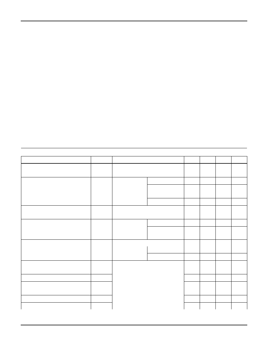
Absolute Maximum Ratings TC = 25oC, Unless Otherwise Specified
ALL TYPES
UNITS
Collector to Emitter Voltage . . . . . . . . . . . . . . . . . . . . . . . . . . . . . . . . . . . . . . . . . . . . . . BVCES
600
V
Collector Current Continuous
At TC = 25
oC . . . . . . . . . . . . . . . . . . . . . . . . . . . . . . . . . . . . . . . . . . . . . . . . . . . . . . . . . I
C25
14
A
At TC = 110
oC . . . . . . . . . . . . . . . . . . . . . . . . . . . . . . . . . . . . . . . . . . . . . . . . . . . . . . . I
C110
7A
Collector Current Pulsed (Note 1) . . . . . . . . . . . . . . . . . . . . . . . . . . . . . . . . . . . . . . . . . . . ICM
56
A
Gate to Emitter Voltage Continuous. . . . . . . . . . . . . . . . . . . . . . . . . . . . . . . . . . . . . . . . . VGES
±20
V
Gate to Emitter Voltage Pulsed . . . . . . . . . . . . . . . . . . . . . . . . . . . . . . . . . . . . . . . . . . . . VGEM
±30
V
Switching Safe Operating Area at TJ = 150
oC, Figure 2 . . . . . . . . . . . . . . . . . . . . . . . . SSOA
35A at 600V
Power Dissipation Total at TC = 25
oC . . . . . . . . . . . . . . . . . . . . . . . . . . . . . . . . . . . . . . . . . P
D
60
W
Power Dissipation Derating TC > 25
oC . . . . . . . . . . . . . . . . . . . . . . . . . . . . . . . . . . . . . . . . . .
0.476
W/oC
Reverse Voltage Avalanche Energy . . . . . . . . . . . . . . . . . . . . . . . . . . . . . . . . . . . . . . . . . EARV
100
mJ
Operating and Storage Junction Temperature Range . . . . . . . . . . . . . . . . . . . . . . . . TJ, TSTG
-55 to 150
oC
Maximum Lead Temperature for Soldering . . . . . . . . . . . . . . . . . . . . . . . . . . . . . . . . . . . . . TL
260
oC
Short Circuit Withstand Time (Note 2) at VGE = 15V. . . . . . . . . . . . . . . . . . . . . . . . . . . . . . tSC
2
s
Short Circuit Withstand Time (Note 2) at VGE = 10V. . . . . . . . . . . . . . . . . . . . . . . . . . . . . . tSC
12
s
CAUTION: Stresses above those listed in “Absolute Maximum Ratings” may cause permanent damage to the device. This is a stress only rating and operation of the
device at these or any other conditions above those indicated in the operational sections of this specification is not implied.
NOTES:
1. Single Pulse; Pulse width limited by maximum junction temperature. Parts may current limit at less than ICM.
2. VCE = 360V, TJ = 125
oC, R
G = 50 .
Electrical Specifications
TC = 25
oC, Unless Otherwise Specified
PARAMETER
SYMBOL
TEST CONDITIONS
MIN
TYP
MAX
UNITS
Collector to Emitter Breakdown Voltage
BVCES
IC = 250A, VGE = 0V
600
-
V
Emitter to Collector Breakdown Voltage
BVECS
IC = 3mA, VGE = 0V
15
28
-
V
Collector to Emitter Leakage Current
ICES
VCE = BVCES
TC = 25
oC
-
100
A
TC = 150
oC-
-
2.0
mA
Collector to Emitter Saturation Voltage
VCE(SAT)
IC = IC110,
VGE = 15V
TC = 25
oC-
1.8
2.1
V
TC = 150
oC-
2.1
2.4
V
Gate to Emitter Threshold Voltage
VGE(TH)
IC = 250A, VCE = VGE
3.0
5.1
6.0
V
Gate to Emitter Leakage Current
IGES
VGE = ±20V
-
±100
nA
Switching SOA
SSOA
TJ = 150
oC
RG = 50
VGE = 15V
L = 100
H
VCE = 480V
42
-
A
VCE = 600V
35
-
A
Gate to Emitter Plateau Voltage
VGEP
IC = IC110, VCE = 0.5 BVCES
-7.7
-
V
On-State Gate Charge
QG(ON)
IC = IC110,
VCE = 0. 5BVCES
VGE = 15V
-
23
28
nC
VGE = 20V
-
30
37
nC
Current Turn-On Delay Time
td(ON)I
IGBT and Diode Both at TJ = 25
oC
ICE = IC110, VCE = 0.8 BVCES,
VGE = 15V, RG = 50, L = 2mH
Test Circuit (Figure 17)
-26-
ns
Current Rise Time
trI
-21-
ns
Current Turn-Off Delay Time
td(OFF)I
-
130
160
ns
Current Fall Time
tfI
-60
80
ns
Turn-On Energy (Note 4)
EON1
-72-
J
Turn-On Energy (Note 4)
EON2
-
160
200
J
Turn-Off Energy (Note 3)
EOFF
-
120
200
J
HGTD7N60B3S, HGT1S7N60B3S, HGTP7N60B3
相关PDF资料 |
PDF描述 |
|---|---|
| HGTD7N60B3S9A | 14 A, 600 V, N-CHANNEL IGBT |
| HHS45-033-0C | 1-OUTPUT DC-DC REG PWR SUPPLY MODULE |
| HHSC-105-06.00-SE-SU | INTERCONNECTION DEVICE |
| HHSC-125-03.75-SE-TE | INTERCONNECTION DEVICE |
| HHSC-108-03.75-TU-SU | INTERCONNECTION DEVICE |
相关代理商/技术参数 |
参数描述 |
|---|---|
| HGT1S7N60C3D | 功能描述:IGBT 晶体管 Optocoupler Phototransistor RoHS:否 制造商:Fairchild Semiconductor 配置: 集电极—发射极最大电压 VCEO:650 V 集电极—射极饱和电压:2.3 V 栅极/发射极最大电压:20 V 在25 C的连续集电极电流:150 A 栅极—射极漏泄电流:400 nA 功率耗散:187 W 最大工作温度: 封装 / 箱体:TO-247 封装:Tube |
| HGT1S7N60C3DS | 功能描述:IGBT 晶体管 7A 600V TF=275NS RoHS:否 制造商:Fairchild Semiconductor 配置: 集电极—发射极最大电压 VCEO:650 V 集电极—射极饱和电压:2.3 V 栅极/发射极最大电压:20 V 在25 C的连续集电极电流:150 A 栅极—射极漏泄电流:400 nA 功率耗散:187 W 最大工作温度: 封装 / 箱体:TO-247 封装:Tube |
| HGT1S7N60C3DS9A | 功能描述:IGBT 晶体管 14a 600V N-Ch IGBT UFS Series RoHS:否 制造商:Fairchild Semiconductor 配置: 集电极—发射极最大电压 VCEO:650 V 集电极—射极饱和电压:2.3 V 栅极/发射极最大电压:20 V 在25 C的连续集电极电流:150 A 栅极—射极漏泄电流:400 nA 功率耗散:187 W 最大工作温度: 封装 / 箱体:TO-247 封装:Tube |
| HGT1Y40N60B3D | 制造商:FAIRCHILD 制造商全称:Fairchild Semiconductor 功能描述:70A, 600V, UFS Series N-Channel IGBT with Anti-Parallel Hyperfast Diodes |
| HGT1Y40N60C3D | 制造商:未知厂家 制造商全称:未知厂家 功能描述:TRANSISTOR | IGBT | N-CHAN | 600V V(BR)CES | 40A I(C) | TO-264 |
发布紧急采购,3分钟左右您将得到回复。