参数资料
| 型号: | HI5805BIB |
| 厂商: | Intersil |
| 文件页数: | 11/12页 |
| 文件大小: | 0K |
| 描述: | IC ADC 12-BIT 5MSPS 28-SOIC |
| 标准包装: | 26 |
| 位数: | 12 |
| 采样率(每秒): | 5M |
| 数据接口: | 并联 |
| 转换器数目: | 3 |
| 功率耗散(最大): | 350mW |
| 电压电源: | 模拟和数字 |
| 工作温度: | -40°C ~ 85°C |
| 安装类型: | 表面贴装 |
| 封装/外壳: | 28-SOIC(0.295",7.50mm 宽) |
| 供应商设备封装: | 28-SOIC W |
| 包装: | 管件 |
| 输入数目和类型: | 2 个单端,单极;1 个差分,双极 |
8
Detailed Description
Theory of Operation
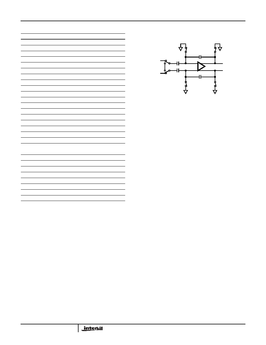
The HI5805 is a 12-bit, fully-differential, sampling pipeline A/D
converter with digital error correction. Figure 14 depicts the
circuit for the front end differential-in-differential-out sample-
and-hold (S/H). The switches are controlled by an internal
clock which is a non-overlapping two phase signal, f1 and f2,
derived from the master clock. During the sampling phase, f1,
the input signal is applied to the sampling capacitors, CS. At
the same time the holding capacitors, CH, are discharged to
analog ground. At the falling edge of f1 the input signal is
sampled on the bottom plates of the sampling capacitors. In
the next clock phase, f2, the two bottom plates of the
sampling capacitors are connected together and the holding
capacitors are switched to the op-amp output nodes. The
charge then redistributes between CS and CH completing one
sample-and-hold cycle. The output is a fully-differential,
sampled-data representation of the analog input. The circuit
not only performs the sample-and-hold function but will also
convert a single-ended input to a fully-differential output for
the converter core. During the sampling phase, the VIN pins
see only the on-resistance of a switch and CS. The relatively
small values of these components result in a typical full power
input bandwidth of 100MHz for the converter.
As illustrated in the functional block diagram and the timing
diagram in Figure 1, three identical pipeline subconverter
stages, each containing a four-bit flash converter, a four-bit
digital-to-analog converter and an amplifier with a voltage
gain of 8, follow the S/H circuit with the fourth stage being
only a 4-bit flash converter. Each converter stage in the
pipeline will be sampling in one phase and amplifying in the
other clock phase. Each individual sub-converter clock
signal is offset by 180 degrees from the previous stage
clock signal, with the result that alternate stages in the
pipeline will perform the same operation.
The 4-bit digital output of each stage is fed to a digital delay
line controlled by the internal clock. The purpose of the delay
line is to align the digital output data to the corresponding
sampled analog input signal. This delayed data is fed to the
digital error correction circuit which corrects the error in the
output data with the information contained in the redundant
bits to form the final 12-bit output for the converter.
Because of the pipeline nature of this converter, the data on
the bus is output at the 3rd cycle of the clock after the analog
sample is taken. This delay is specified as the data latency.
After the data latency time, the data representing each
succeeding sample is output at the following clock pulse. The
output data is synchronized to the external clock by a latch.
The digital outputs are in offset binary format (See Table 1).
Internal Reference Generator, VROUT and VRIN
The HI5805 has an internal reference generator, therefore, no
external reference voltage is required. VROUT must be
connected to VRIN when using the internal reference voltage.
The HI5805 can be used with an external reference. The
converter requires only one external reference voltage
connected to the VRIN pin with VROUT left open.
The HI5805 is tested with VRIN equal to 3.5V. Internal to the
converter, two reference voltages of 1.3V and 3.3V are
generated for a fully differential input signal range of
±2V.
In order to minimize overall converter noise, it is
recommended that adequate high frequency decoupling be
provided at the reference voltage input pin, VRIN.
Pin Descriptions
PIN NO.
NAME
DESCRIPTION
1
CLK
Input Clock.
2
DVCC1
Digital Supply (5.0V).
3
DGND1
Digital Ground.
4
DVCC1
Digital Supply (5.0V).
5
DGND1
Digital Ground
6
AVCC
Analog Supply (5.0V).
7
AGND
Analog Ground.
8
VIN+
Positive Analog Input.
9
VIN-
Negative Analog Input.
10
VDC
DC Bias Voltage Output.
11
VROUT
Reference Voltage Output.
12
VRIN
Reference Voltage Input.
13
AGND
Analog Ground.
14
AVCC
Analog Supply (5.0V).
15
D11
Data Bit 11 Output (MSB).
16
D10
Data Bit 10 Output.
17
D9
Data Bit 9 Output.
18
D8
Data Bit 8 Output.
19
D7
Data Bit 7 Output.
20
D6
Data Bit 6 Output.
21
DGND2
Digital Output Ground.
22
DVCC2
Digital Output Supply (3.0V to 5.0V).
23
D5
Data Bit 5 Output.
24
D4
Data Bit 4 Output.
25
D3
Data Bit 3 Output.
26
D2
Data Bit 2 Output.
27
D1
Data Bit 1 Output.
28
D0
Data Bit 0 Output (LSB).
CH
CS
VIN+
VOUT+
VOUT -
VIN-
φ
1
φ
1
φ
2
φ
1
φ
1
CH
φ
1
φ
1
FIGURE 14. ANALOG INPUT SAMPLE-AND-HOLD
+
-
- +
HI5805
相关PDF资料 |
PDF描述 |
|---|---|
| HI5812JIBZ-T | ADC 12BIT SAMPL TRK&HOLD 24-SOIC |
| HI5828IN | DAC DUAL 12BIT 130MHZ 48-LQFP |
| HI5860IBZ | CONV D/A 12-BIT 130MSPS 28-SOIC |
| HI5960IAZ | CONV D/A 14BIT 130MSPS 28-TSSOP |
| HI7188IN | CONV A/D 16BIT 8:1 MUX 44-MQFP |
相关代理商/技术参数 |
参数描述 |
|---|---|
| HI5805BIBZ | 功能描述:模数转换器 - ADC 28 INDTEMP A/D 12BIT 5MSPS 0 5LSB V-REF RoHS:否 制造商:Texas Instruments 通道数量:2 结构:Sigma-Delta 转换速率:125 SPs to 8 KSPs 分辨率:24 bit 输入类型:Differential 信噪比:107 dB 接口类型:SPI 工作电源电压:1.7 V to 3.6 V, 2.7 V to 5.25 V 最大工作温度:+ 85 C 安装风格:SMD/SMT 封装 / 箱体:VQFN-32 |
| HI5805EVAL1 | 功能描述:数据转换 IC 开发工具 HI5805 EVAL PL ATFORM RoHS:否 制造商:Texas Instruments 产品:Demonstration Kits 类型:ADC 工具用于评估:ADS130E08 接口类型:SPI 工作电源电压:- 6 V to + 6 V |
| HI5806IB | 制造商:Rochester Electronics LLC 功能描述:- Bulk |
| HI5808 | 制造商:INTERSIL 制造商全称:Intersil Corporation 功能描述:12-Bit, 9MSPS A/D Converter |
| HI5808_01 | 制造商:INTERSIL 制造商全称:Intersil Corporation 功能描述:12-Bit, 9MSPS A/D Converter |
发布紧急采购,3分钟左右您将得到回复。