参数资料
| 型号: | HI5805BIB |
| 厂商: | Intersil |
| 文件页数: | 2/12页 |
| 文件大小: | 0K |
| 描述: | IC ADC 12-BIT 5MSPS 28-SOIC |
| 标准包装: | 26 |
| 位数: | 12 |
| 采样率(每秒): | 5M |
| 数据接口: | 并联 |
| 转换器数目: | 3 |
| 功率耗散(最大): | 350mW |
| 电压电源: | 模拟和数字 |
| 工作温度: | -40°C ~ 85°C |
| 安装类型: | 表面贴装 |
| 封装/外壳: | 28-SOIC(0.295",7.50mm 宽) |
| 供应商设备封装: | 28-SOIC W |
| 包装: | 管件 |
| 输入数目和类型: | 2 个单端,单极;1 个差分,双极 |
10
Again, the difference between the two internal voltage
references is 2V. If VIN is a 4VP-P sinewave, then VIN+ is a
4VP-P sinewave riding on a positive voltage equal to VDC.
The converter will be at positive full scale when VIN+ is at
VDC + 2V (VIN+ - VIN- = 2V) and will be at negative full scale
when VIN+ is equal to VDC - 2V (VIN+ - VIN- = -2V). In this
case, VDC could range between 2V and 3V without a
significant change in ADC performance. The simplest way to
produce VDC is to use the VDC bias voltage output of the
HI5805.
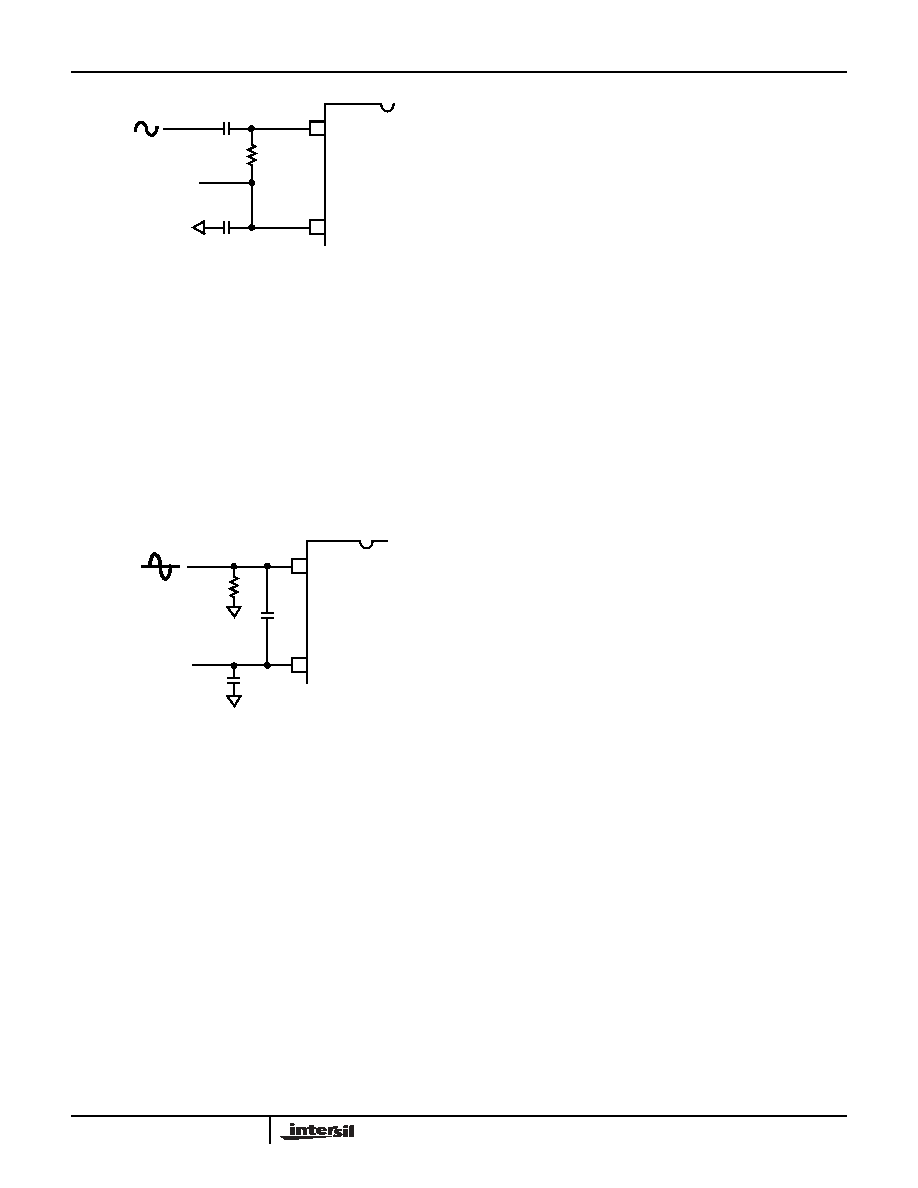
The single ended analog input can be DC coupled (Figure
18) as long as the input is within the analog input common
mode voltage range.
The resistor, R, in Figure 18 is not absolutely necessary but
may be used as a load setting resistor. A capacitor, C,
connected from VIN+ to VIN- will help filter any high
frequency noise on the inputs, also improving performance.
Values around 20pF are sufficient and can be used on AC
coupled inputs as well. Note, however, that the value of
capacitor C chosen must take into account the highest
frequency component of the analog input signal.
A single ended source will give better overall system
performance if it is first converted to differential before
driving the HI5805.
Digital I/O and Clock Requirements
The HI5805 provides a standard high-speed interface to
external TTL/CMOS logic families. The digital CMOS clock
input has TTL level thresholds. The low input bias current
allows the HI5805 to be driven by CMOS logic.
The digital CMOS outputs have a separate digital supply.
This allows the digital outputs to operate from a 3.0V to 5.0V
supply. When driving CMOS logic, the digital outputs will
swing to the rails. When driving standard TTL loads, the
digital outputs will meet standard TTL level requirements
even with a 3.0V supply.
In order to ensure rated performance of the HI5805, the duty
cycle of the clock should be held at 50%
±5%. It must also
have low jitter and operate at standard TTL levels.
Performance of the HI5805 will only be guaranteed at
conversion rates above 0.5MSPS. This ensures proper
performance of the internal dynamic circuits.
Supply and Ground Considerations
The HI5805 has separate analog and digital supply and
ground pins to keep digital noise out of the analog signal
path. The part should be mounted on a board that provides
separate low impedance connections for the analog and
digital supplies and grounds. For best performance, the
supplies to the HI5805 should be driven by clean, linear
regulated supplies. The board should also have good high
frequency decoupling capacitors mounted as close as
possible to the converter. If the part is powered off a single
supply then the analog supply and ground pins should be
isolated by ferrite beads from the digital supply and ground
pins.
Refer to the Application Note AN9214, “Using Intersil High
Speed A/D Converters” for additional considerations when
using high speed converters.
Static Performance Definitions
Offset Error (VOS)
The midscale code transition should occur at a level 1/4 LSB
above half scale. Offset is defined as the deviation of the
actual code transition from this point.
Full-Scale Error (FSE)
The last code transition should occur for an analog input that
is 3/4 LSB below positive full scale with the offset error
removed. Full-scale error is defined as the deviation of the
actual code transition from this point.
Differential Linearity Error (DNL)
DNL is the worst case deviation of a code width from the
ideal value of 1 LSB.
Integral Linearity Error (INL)
INL is the worst case deviation of a code center from a best
fit straight line calculated from the measured data.
Power Supply Rejection Ratio (PSRR)
Each of the power supplies are moved plus and minus 5%
and the shift in the offset and gain error (in LSBs) is noted.
VIN+
VIN-
HI5805
VIN
VDC
FIGURE 17. AC COUPLED SINGLE ENDED INPUT
VIN+
VIN-
HI5805
VDC
R
C
VIN
VDC
FIGURE 18. DC COUPLED SINGLE ENDED INPUT
HI5805
相关PDF资料 |
PDF描述 |
|---|---|
| HI5812JIBZ-T | ADC 12BIT SAMPL TRK&HOLD 24-SOIC |
| HI5828IN | DAC DUAL 12BIT 130MHZ 48-LQFP |
| HI5860IBZ | CONV D/A 12-BIT 130MSPS 28-SOIC |
| HI5960IAZ | CONV D/A 14BIT 130MSPS 28-TSSOP |
| HI7188IN | CONV A/D 16BIT 8:1 MUX 44-MQFP |
相关代理商/技术参数 |
参数描述 |
|---|---|
| HI5805BIBZ | 功能描述:模数转换器 - ADC 28 INDTEMP A/D 12BIT 5MSPS 0 5LSB V-REF RoHS:否 制造商:Texas Instruments 通道数量:2 结构:Sigma-Delta 转换速率:125 SPs to 8 KSPs 分辨率:24 bit 输入类型:Differential 信噪比:107 dB 接口类型:SPI 工作电源电压:1.7 V to 3.6 V, 2.7 V to 5.25 V 最大工作温度:+ 85 C 安装风格:SMD/SMT 封装 / 箱体:VQFN-32 |
| HI5805EVAL1 | 功能描述:数据转换 IC 开发工具 HI5805 EVAL PL ATFORM RoHS:否 制造商:Texas Instruments 产品:Demonstration Kits 类型:ADC 工具用于评估:ADS130E08 接口类型:SPI 工作电源电压:- 6 V to + 6 V |
| HI5806IB | 制造商:Rochester Electronics LLC 功能描述:- Bulk |
| HI5808 | 制造商:INTERSIL 制造商全称:Intersil Corporation 功能描述:12-Bit, 9MSPS A/D Converter |
| HI5808_01 | 制造商:INTERSIL 制造商全称:Intersil Corporation 功能描述:12-Bit, 9MSPS A/D Converter |
发布紧急采购,3分钟左右您将得到回复。