- 您现在的位置:买卖IC网 > PDF目录384468 > HY5PS1G831CLFP-Y5 (HYNIX SEMICONDUCTOR INC) 1Gb DDR2 SDRAM PDF资料下载
参数资料
| 型号: | HY5PS1G831CLFP-Y5 |
| 厂商: | HYNIX SEMICONDUCTOR INC |
| 元件分类: | DRAM |
| 英文描述: | 1Gb DDR2 SDRAM |
| 中文描述: | 128M X 8 DDR DRAM, 0.45 ns, PBGA60 |
| 封装: | ROHS COMPLIANT, FBGA-60 |
| 文件页数: | 8/37页 |
| 文件大小: | 539K |
| 代理商: | HY5PS1G831CLFP-Y5 |
第1页第2页第3页第4页第5页第6页第7页当前第8页第9页第10页第11页第12页第13页第14页第15页第16页第17页第18页第19页第20页第21页第22页第23页第24页第25页第26页第27页第28页第29页第30页第31页第32页第33页第34页第35页第36页第37页
Rev. 0.2 / Dec 2006
8
HY5PS1G431C(L)FP
HY5PS1G831C(L)FP
HY5PS1G1631C(L)FP
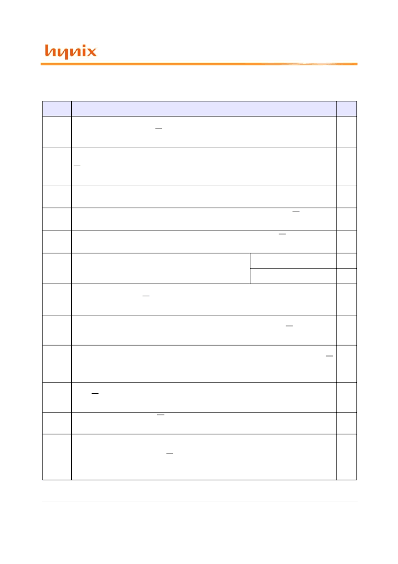
IDD Test Conditions
(IDD values are for full operating range of Voltage and Temperature, Notes 1-5)
Symbol
Conditions
Units
IDD0
Operating one bank active-precharge current
; tCK = tCK(IDD), tRC = tRC(IDD), tRAS =
tRAS min(IDD) ; CKE is HIGH, CS is HIGH between valid commands;Address bus inputs are
SWITCHING;Data bus inputs are SWITCHING
mA
IDD1
Operating one bank active-read-precharge current
; IOUT = 0mA;BL = 4, CL = CL(IDD), AL
= 0; tCK = tCK(IDD), tRC = tRC (IDD), tRAS = tRASmin(IDD), tRCD = tRCD(IDD) ; CKE is HIGH,
CS is HIGH between valid commands ; Address bus inputs are SWITCHING ; Data pattern is same
as IDD4W
mA
IDD2P
Precharge power-down current
; All banks idle ; tCK = tCK(IDD) ; CKE is LOW ; Other control
and address bus inputs are STABLE; Data bus inputs are FLOATING
mA
IDD2Q
Precharge quiet standby current
;All banks idle; tCK = tCK(IDD);CKE is HIGH, CS is HIGH;
Other control and address bus inputs are STABLE; Data bus inputs are FLOATING
mA
IDD2N
Precharge standby current
; All banks idle; tCK = tCK(IDD); CKE is HIGH, CS is HIGH; Other
control and address bus inputs are SWITCHING; Data bus inputs are SWITCHING
mA
IDD3P
Active power-down current
; All banks open; tCK = tCK(IDD);
CKE is LOW; Other control and address bus inputs are STABLE;
Data bus inputs are FLOATING
Fast PDN Exit MRS(12) = 0
mA
Slow PDN Exit MRS(12) = 1
mA
IDD3N
Active standby current
; All banks open; tCK = tCK(IDD), tRAS = tRASmax(IDD), tRP
=tRP(IDD); CKE is HIGH, CS is HIGH between valid commands; Other control and address bus
inputs are SWITCHING; Data bus inputs are SWITCHING
mA
IDD4W
Operating burst write current
; All banks open, Continuous burst writes; BL = 4, CL = CL(IDD),
AL = 0; tCK = tCK(IDD), tRAS = tRASmax(IDD), tRP = tRP(IDD); CKE is HIGH, CS is HIGH
between valid commands; Address bus inputs are SWITCHING; Data bus inputs are SWITCHING
mA
IDD4R
Operating burst read current
; All banks open, Continuous burst reads, IOUT = 0mA; BL = 4,
CL = CL(IDD), AL = 0; tCK = tCK(IDD), tRAS = tRASmax(IDD), tRP = tRP(IDD); CKE is HIGH, CS
is HIGH between valid commands; Address bus inputs are SWITCHING;; Data pattern is same as
IDD4W
mA
IDD5B
Burst refresh current
; tCK = tCK(IDD); Refresh command at every tRFC(IDD) interval; CKE is
HIGH, CS is HIGH between valid commands; Other control and address bus inputs are SWITCH-
ING; Data bus inputs are SWITCHING
mA
IDD6
Self refresh current
; CK and CK at 0V; CKE £ 0.2V; Other control and address bus inputs are
FLOATING; Data bus inputs are FLOATING
mA
IDD7
Operating bank interleave read current
; All bank interleaving reads, IOUT = 0mA; BL = 4, CL
= CL(IDD), AL = tRCD(IDD)-1*tCK(IDD); tCK = tCK(IDD), tRC = tRC(IDD), tRRD = tRRD(IDD),
tRCD = 1*tCK(IDD); CKE is HIGH, CS is HIGH between valid commands; Address bus inputs are
STABLE during DESELECTs; Data pattern is same as IDD4R; - Refer to the following page for
detailed timing conditions
mA
相关PDF资料 |
PDF描述 |
|---|---|
| HY5PS1G821LM-E3 | 1Gb DDR2 SDRAM(DDP) |
| HY5PS1G821M | 1Gb DDR2 SDRAM(DDP) |
| HY5PS1G821M-C4 | 1Gb DDR2 SDRAM(DDP) |
| HY5PS1G821M-E3 | 1Gb DDR2 SDRAM(DDP) |
| HY5PS1G421LM | 1Gb DDR2 SDRAM(DDP) |
相关代理商/技术参数 |
参数描述 |
|---|---|
| HY5PS1G831F | 制造商:HYNIX 制造商全称:Hynix Semiconductor 功能描述:1Gb DDR2 SDRAM |
| HY5PS1G831F-C4 | 制造商:HYNIX 制造商全称:Hynix Semiconductor 功能描述:1Gb DDR2 SDRAM |
| HY5PS1G831F-C5 | 制造商:HYNIX 制造商全称:Hynix Semiconductor 功能描述:1Gb DDR2 SDRAM |
| HY5PS1G831F-E3 | 制造商:HYNIX 制造商全称:Hynix Semiconductor 功能描述:1Gb DDR2 SDRAM |
| HY5PS1G831F-E4 | 制造商:HYNIX 制造商全称:Hynix Semiconductor 功能描述:1Gb DDR2 SDRAM |
发布紧急采购,3分钟左右您将得到回复。