- 您现在的位置:买卖IC网 > PDF目录175503 > HYMD264646A8J-D43 (HYNIX SEMICONDUCTOR INC) 64M X 64 DDR DRAM MODULE, 0.7 ns, DMA184 PDF资料下载
参数资料
| 型号: | HYMD264646A8J-D43 |
| 厂商: | HYNIX SEMICONDUCTOR INC |
| 元件分类: | DRAM |
| 英文描述: | 64M X 64 DDR DRAM MODULE, 0.7 ns, DMA184 |
| 封装: | 5.250 X 1.250 X 0.150 INCH, DIMM-184 |
| 文件页数: | 5/18页 |
| 文件大小: | 227K |
| 代理商: | HYMD264646A8J-D43 |
HYMD264646A8J
Rev. 0.3 / June. 2003
13
8.
Minimum of 200 cycles of stable input clocks after Self Refresh Exit command, where CKE is held high, is required to complete
Self Refresh Exit and lock the internal DLL circuit of DDR SDRAM.
9.
Min (tCL, tCH) refers to the smaller of the actual clock low time and the actual clock high time as provided to the device
(i.e. this value can be greater than the minimum specification limits for tCL and tCH).
10. tHP = minimum half clock period for any given cycle and is defined by clock high or clock low (tCH, tCL). tQHS consists of
tDQSQmax, the pulse width distortion of on-chip clock circuits, data pin to pin skew and output pattern effects and p-channel
to n-channel variation of the output drivers.
11
. This derating table is used to increase tDS/tDH in case where the input slew-rate is below 0.5V/ns.
Input Setup / Hold Slew-rate Derating Table.
12.
I/O Setup/Hold Plateau Derating. This derating table is used to increase tDS/tDH in case where the input level is flat below
VREF +/-310mV for a duration of up to 2ns.
13.
I/O Setup/Hold Delta Inverse Slew Rate Derating. This derating table is used to increase tDS/tDH in case where the DQ and
DQS slew rates differ. The Delta Inverse Slew Rate is calculated as (1/SlewRate1)-(1/SlewRate2). For example, if slew rate
1=0.5V/ns and Slew Rate2 = 0.4V/n then the Delta Inverse Slew Rate = -0.5ns/V.
14.
DQS, DM and DQ input slew rate is specified to prevent double clocking of data and preserve setup and hold times.
Signal transi tions through the DC region must be monotonic.
15.
tDAL = (tDPL / tCK ) + (tRP / tCK ). For each of the terms above, if not already an integer, round to the next highest integer.
tCK is equal to the actual system clock cycle time.
Example: For DDR266B at CL=2.5 and tCK = 7.5 ns,
tDAL = (15 ns / 7.5 ns) + (20 ns / 7.5 ns) = (2.00) + (2.67)
Round up each non-integer to the next highest integer: = (2) + (3), tDAL = 5 clock
16.
For the parts which do not has internal RAS lockout circuit, Active to Read with Auto precharge delay should be
tRAS - BL/2 x tCK.
17.
tHZ and tLZ transitions occur in the same access time windows as valid data trasitions. These parameters are not referenced
to a specific voltage level but specify when the device output is no longer driving (HZ), or begins driving (LZ).
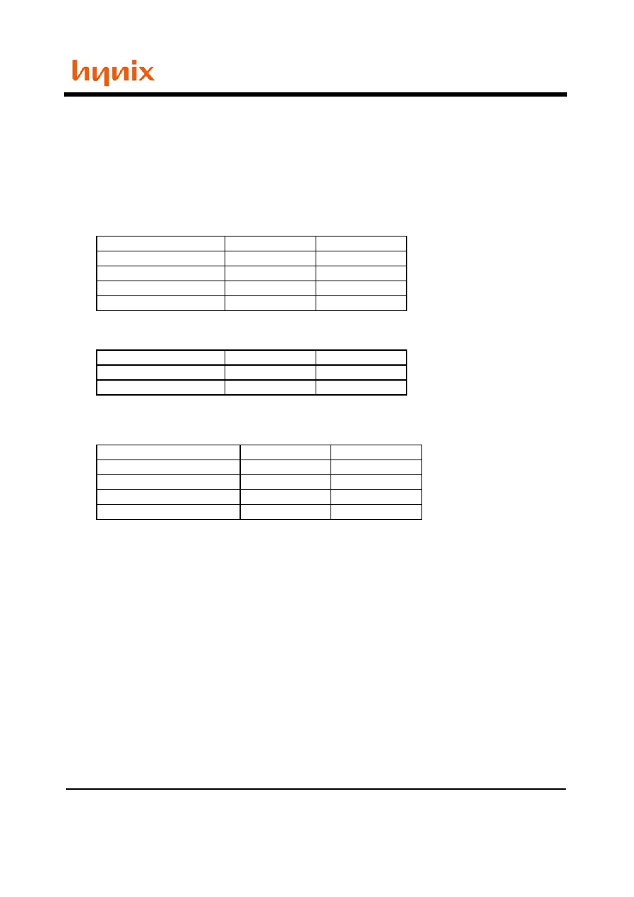
Input Setup / Hold Slew-rate
Delta tDS
Delta tDH
V/ns
ps
0.5
0
0.4
+75
0.3
+150
I/O Input Level
Delta tDS
Delta tDH
mV
ps
+280
+50
(1/SlewRate1)-(1/SlewRate2)
Delta tDS
Delta tDH
ns/V
ps
00
0
+/-0.25
+50
+/- 0.5
+100
相关PDF资料 |
PDF描述 |
|---|---|
| HYS72V64220GU-7.5-C | 64M X 72 SYNCHRONOUS DRAM MODULE, 5.4 ns, DMA168 |
| HZ11C1LRH | 0.4 W, SILICON, UNIDIRECTIONAL VOLTAGE REGULATOR DIODE, DO-35 |
| HZ33-2LTA | 0.4 W, SILICON, UNIDIRECTIONAL VOLTAGE REGULATOR DIODE, DO-35 |
| HZ36-1LTD | 0.4 W, SILICON, UNIDIRECTIONAL VOLTAGE REGULATOR DIODE, DO-35 |
| HZ36-3LTD | 0.4 W, SILICON, UNIDIRECTIONAL VOLTAGE REGULATOR DIODE, DO-35 |
相关代理商/技术参数 |
参数描述 |
|---|---|
| HYMD264646A8J-J | 制造商:HYNIX 制造商全称:Hynix Semiconductor 功能描述:Unbuffered DDR SDRAM DIMM |
| HYMD264646A8-K | 制造商:HYNIX 制造商全称:Hynix Semiconductor 功能描述:Unbuffered DDR SDRAM DIMM |
| HYMD264646A8-L | 制造商:HYNIX 制造商全称:Hynix Semiconductor 功能描述:Unbuffered DDR SDRAM DIMM |
| HYMD264646A8-M | 制造商:HYNIX 制造商全称:Hynix Semiconductor 功能描述:Unbuffered DDR SDRAM DIMM |
| HYMD264646AL8 | 制造商:未知厂家 制造商全称:未知厂家 功能描述:64Mx64|2.5V|M/K/H/L|x16|DDR SDRAM - Unbuffered DIMM 512MB |
发布紧急采购,3分钟左右您将得到回复。