- 您现在的位置:买卖IC网 > PDF目录67682 > IBM25PPC405GPR3BB400Z 32-BIT, 400 MHz, RISC PROCESSOR, PBGA456 PDF资料下载
参数资料
| 型号: | IBM25PPC405GPR3BB400Z |
| 元件分类: | 微控制器/微处理器 |
| 英文描述: | 32-BIT, 400 MHz, RISC PROCESSOR, PBGA456 |
| 封装: | 35 X 35 MM, ENHANCED, PLASTIC, BGA-456 |
| 文件页数: | 26/58页 |
| 文件大小: | 1264K |
| 代理商: | IBM25PPC405GPR3BB400Z |
第1页第2页第3页第4页第5页第6页第7页第8页第9页第10页第11页第12页第13页第14页第15页第16页第17页第18页第19页第20页第21页第22页第23页第24页第25页当前第26页第27页第28页第29页第30页第31页第32页第33页第34页第35页第36页第37页第38页第39页第40页第41页第42页第43页第44页第45页第46页第47页第48页第49页第50页第51页第52页第53页第54页第55页第56页第57页第58页
Preliminary
PowerPC 405GPr Embedded Processor Data Sheet
Page 32 of 58
3/14/03
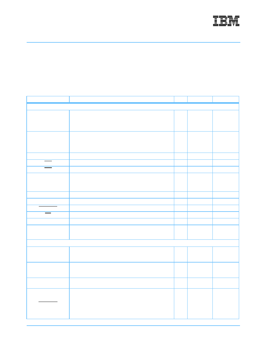
SDRAM Interface
MemData0:31
Memory data bus.
Notes:
1. MemData0 is the most significant bit (msb).
2. MemData31 is the least significant bit (lsb).
I/O
3.3V LVTTL
MemAddr12:0
Memory address bus.
Notes:
1. MemAddr12 is the most significant bit (msb).
2. MemAddr0 is the least significant bit (lsb).
O3.3V LVTTL
BA1:0
Bank Address supporting up to 4 internal banks.
O
3.3V LVTTL
RAS
Row Address Strobe.
O
3.3V LVTTL
CAS
Column Address Strobe.
O
3.3V LVTTL
DQM0:3
DQM for byte lane: 0 (MemData0:7),
1 (MemData8:15),
2 (MemData16:23), and
3 (MemData24:31)
O3.3V LVTTL
DQMCB
DQM for ECC check bits.
O
3.3V LVTTL
ECC0:7
ECC check bits 0:7.
I/O
3.3V LVTTL
BankSel0:3
Select up to four external SDRAM banks.
O
3.3V LVTTL
WE
Write Enable.
O
3.3V LVTTL
ClkEn0:1
SDRAM Clock Enable.
O
3.3V LVTTL
MemClkOut0:1
Two copies of an SDRAM clock allows, in some cases, glueless
SDRAM attach without requiring this signal to be repowered by a
PLL or zero-delay buffer.
O3.3V LVTTL
External Slave Peripheral Interface
PerData0:31
Peripheral data bus used by PPC405GPr when not in external
master mode, otherwise used by external master.
Note: PerData0 is the most significant bit (msb) on this bus.
I/O
5V tolerant
3.3V LVTTL
1
PerAddr0:31
Peripheral address bus used by PPC405GPr when not in external
master mode, otherwise used by external master.
Note: PerAddr0 is the most significant bit (msb) on this bus.
I/O
5V tolerant
3.3V LVTTL
1
PerPar0:3
Peripheral byte parity signals.
I/O
5V tolerant
3.3V LVTTL
1
PerWBE0:3
As outputs, these pins can act as byte-enables which are valid for
an entire cycle or as write-byte-enables which are valid for each
byte on each data transfer, allowing partial word transactions. As
outputs, pins are used by either the pripheral controller or the
DMA controller depending upon the type of transfer involved.
Used as inputs when an external bus master owns the external
interface.
I/O
5V tolerant
3.3V LVTTL
1, 7
Signal Functional Description (Part 3 of 8)
Multiplexed signals are shown in brackets following the first signal name assigned to each multiplexed ball.
Notes:
1. Receiver input has hysteresis.
2. Must pull up. See “Pull-Up and Pull-Down Resistors” on page 29 for recommended termination values.
3. Must pull down. See “Pull-Up and Pull-Down Resistors” on page 29 for recommended termination values.
4. If not used, must pull up.
5. If not used, must pull down.
6. Strapping input during reset; pull up or pull down as required.
7. Pull-up may be required. See “External Bus Control Signals” on page 29.
Signal Name
Description
I/OType
Notes
相关PDF资料 |
PDF描述 |
|---|---|
| IBM25PPC405GPR3DB266 | 32-BIT, 266 MHz, RISC PROCESSOR, PBGA456 |
| IBM25PPC603E-BX-133X | 32-BIT, 133 MHz, RISC PROCESSOR, CBGA255 |
| IBM25PPC603EV-FX-233X | 32-BIT, 233 MHz, RISC PROCESSOR, CQFP240 |
| IBM25PPC603EV-FX-225X | 32-BIT, 225 MHz, RISC PROCESSOR, CQFP240 |
| IBM25PPC603EV-BX-233X | 32-BIT, 233 MHz, RISC PROCESSOR, CBGA255 |
相关代理商/技术参数 |
参数描述 |
|---|---|
| IBM25PPC405-GPR-3JB266Z | 制造商:IBM 功能描述: |
| IBM25PPC405GPR-3KB266C | 制造商:IBM 功能描述: |
| IBM25PPC440GX3CB667C | 制造商:IBM 功能描述: |
| IBM25PPC603E-BX-080-X | 制造商:未知厂家 制造商全称:未知厂家 功能描述:32-Bit Microprocessor |
| IBM25PPC603E-BX-100-X | 制造商:未知厂家 制造商全称:未知厂家 功能描述:32-Bit Microprocessor |
发布紧急采购,3分钟左右您将得到回复。