- 您现在的位置:买卖IC网 > PDF目录67685 > ICS1527G-60LFTR PLL BASED CLOCK DRIVER, 2 TRUE OUTPUT(S), 0 INVERTED OUTPUT(S), PDSO16 PDF资料下载
参数资料
| 型号: | ICS1527G-60LFTR |
| 元件分类: | 时钟及定时 |
| 英文描述: | PLL BASED CLOCK DRIVER, 2 TRUE OUTPUT(S), 0 INVERTED OUTPUT(S), PDSO16 |
| 封装: | 4.40 MM, 0.65 MM PITCH, LEAD FREE, TSSOP-16 |
| 文件页数: | 4/11页 |
| 文件大小: | 620K |
| 代理商: | ICS1527G-60LFTR |
MDS 1527 E
2
Revision 060204
Integrated Circuit Systems, 525 Race Street, San Jose, CA 95126, tel (408) 297-1201
www.icst.com
Section 1 Overview
ICS1527 Data Sheet
Section 1 Overview
The ICS1527 is a user-programmable,
high-performance general purpose clock generator. It
is intended for graphics system line-locked and
genlocked applications, and provides the clock signals
required by high-performance analog-to-digital
converters.
The ICS1527 has the ability to operate in line-locked
mode with the HSYNC input.
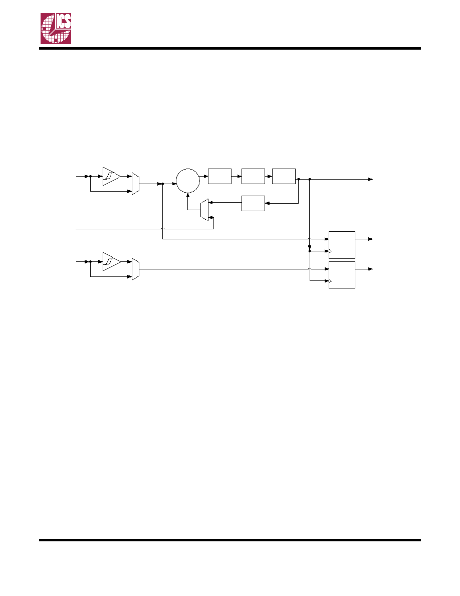
1.1 Phase-Locked Loop
The phase-locked loop has a very wide input frequency
range (8 kHz to 100 MHz). Not only is the ICS1527 an
excellent, general purpose clock synthesizer, but it is
also capable of line-locked operation. Refer to the
block diagram below.
The heart of the ICS1527 is a voltage controlled
oscillator (VCO). The VCO speed is controlled by the
voltage on the loop filter. This voltage will be described
later in this section.
The VCO’s clock output is first passed through the
VCO Divider (VCOD). The VCOD allows the VCO to
operate at higher speeds than the required output
clock.
NOTE: Under normal, locked operation the VCOD has
no effect on the speed of the output clocks, just the
VCO frequency.
The output of the VCOD is the full speed output
frequency seen on the CLK. This clock is then sent
through the 12-bit internal Feedback Divider (FD). The
feedback divider controls how many clocks are seen
during every cycle of the input reference.
The Phase Frequency Detector (PFD) then compares
the feedback to the input and controls the filter voltage
by enabling and disabling the charge pump. The
charge pump has programmable current drive and will
source and sink current as appropriate to keep the
input and the HSYNC_out output aligned.
The input HSYNC and VSYNC can be conditioned by a
high-performance Schmitt-trigger by sharpening the
rising/falling edge.
The HSYNC_out and VSYNC_out signals are aligned
with the output clock (CLK) via a set of flip flops.
1.2 Output Drivers and Logic Inputs
The ICS1527 uses low-voltage TTL (LVTTL) inputs and
LVCMOS outputs, operating at the 3.3 V supply
voltage. The LVTTL inputs are 5 V tolerant.
The LVCMOS drive resistive terminations or
transmission lines.
1.3 Automatic Power-On Reset Detection
The ICS1527 has automatic power-on reset detection
(POR) circuitry and it resets itself if the supply voltage
drops below threshold values. No external connection
to a reset signal is required.
Figure 1-1 Simplified Block Diagram
Note: Polarity controls and other circuit elements are not shown in above diagram for simplicity
PFD
CP
VCO
VCOD
2,4,8,16
HSYNC
Flip-flop
VSYNC
CLK
HSYNC_out
VSYNC_out
FD
12..4103
Flip-flop
EXTFB
相关PDF资料 |
PDF描述 |
|---|---|
| ICS1562BM-001LF | 260 MHz, VIDEO CLOCK GENERATOR, PDSO16 |
| ICS1567M-XXX-LF | 180 MHz, VIDEO CLOCK GENERATOR, PDSO16 |
| ICS1574BM | 130 MHz, VIDEO CLOCK GENERATOR, PDSO16 |
| ICS1890Y-14 | 1 CHANNEL(S), 100M bps, SERIAL COMM CONTROLLER, PQFP64 |
| ICS2059GI-02 | 27 MHz, VIDEO CLOCK GENERATOR, PDSO16 |
相关代理商/技术参数 |
参数描述 |
|---|---|
| ICS1531 | 制造商:ICS 制造商全称:ICS 功能描述:Triple 8-bit MSPS A/D Converters with Line-Locked Clock Generator |
| ICS1532 | 制造商:IDT 制造商全称:Integrated Device Technology 功能描述:110 MHZ TRIPLE 8-BIT ADC WITH CLOCK GENERATOR |
| ICS1560M-001 | 制造商:未知厂家 制造商全称:未知厂家 功能描述:Video/Graphics Clock Generator |
| ICS1560M-003 | 制造商:未知厂家 制造商全称:未知厂家 功能描述:Video/Graphics Clock Generator |
| ICS1560N-001 | 制造商:未知厂家 制造商全称:未知厂家 功能描述:Video/Graphics Clock Generator |
发布紧急采购,3分钟左右您将得到回复。