- 您现在的位置:买卖IC网 > PDF目录175707 > ICS5342-2 Analog IC PDF资料下载
参数资料
| 型号: | ICS5342-2 |
| 英文描述: | Analog IC |
| 中文描述: | 模拟IC |
| 文件页数: | 2/36页 |
| 文件大小: | 1017K |
| 代理商: | ICS5342-2 |
第1页当前第2页第3页第4页第5页第6页第7页第8页第9页第10页第11页第12页第13页第14页第15页第16页第17页第18页第19页第20页第21页第22页第23页第24页第25页第26页第27页第28页第29页第30页第31页第32页第33页第34页第35页第36页
ICS5342
GENDAC
10
tive contents of the color palette RAM to facilitate such oper-
ations as animation and flashing objects. Operations on the
contents of the mask register can also be totally asynchronous
to the pixel stream.
The ICS5342 also includes dual PLL frequency generators
providing a video clock (CLK0) and a memory clock (CLK1),
both generated from a single 14.318 MHz crystal. There are
eight selectable CLK0 frequencies. All eight are programma-
ble. There are two selectable and programmable CLK1 fre-
quencies (fA, fB). Default values (Shown in tables: “Video
Clock Default Frequency Registers,” and “Memory Clock
Default Frequency Registers”) are loaded into the appropriate
registers on power up.
Video Path
The GENDAC supports nine different video modes and is de-
termined by bits 4-7 of the command register. The default
mode is the 8-bit Pseudo Color mode. The other modes are the
bypass 15-bit, 16-bit and 24 bit True Color modes in 8-bit and
16-bit interface, and the 16-bit Pseudo Color (2:1) mode with
2X Clock.
The 24-bit True Color has sparse and packed
modes.
Pseudo Color
8-bit Interface
In this mode, Pixel Address, P7-P0 and BLANK* inputs are
sampled on the rising edge of the clock (PCLK) and any
change appears at the analog outputs after three succeeding
rising edges of the PCLK. The DAC output depends on the
data in the color palette RAM.
16-bit Interface
In this mode, Pixel Address, P15-P0 and BLANK* inputs are
sampled on the rising edge of the clock (PCLK) and any
change appears at the analog outputs after three succeeding
rising edges of the 2 x ICLK. ICLK frequency is twice the
PCLK input frequency. The DAC output depends on the data
in the color palette RAM.
Bypass Mode
The GENDAC supports seven different bypass modes: three
for byte transfers and four for word transfers. In these modes,
the address pins P0-P15 represent Color Data that is applied
directly to the DAC. The internal look-up table RAM is ig-
nored. During byte transfers, the P8-P15 inputs are”don't
care.” Data is always latched on the rising edge of PCLK.
Byte or word framing is internally synchronized with the ris-
ing edge of BLANK*.
DAC Outputs
The outputs of the DACs are designed to be capable of pro-
ducing 0.7 V peak white amplitude with an IREF of 8.88 mA
when driving a doubly-terminated 75
load. This corre-
sponds to an effective DAC output load (REFFECTIVE) of 37.5
. The formula for calculating I
REF with various peak white
voltage/output loading combinations is given below:
Note that for all values of IREF and output loading:
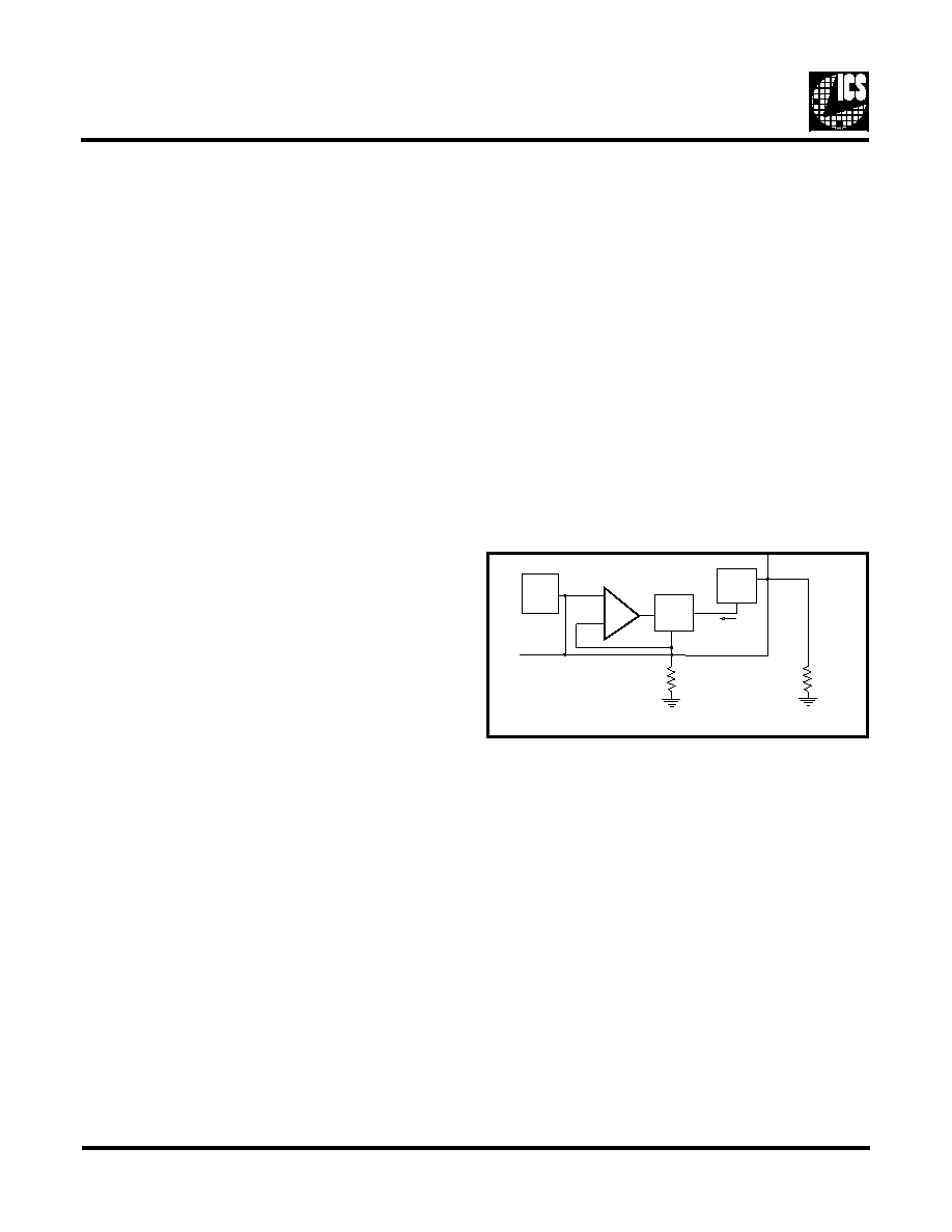
The reference current IREF is determined by the reference
voltage VREF and the value of the resistor connected to RSET
pin. VREF can be the internal band gap reference voltage or
can be overridden by an external voltage. In both cases:
DAC Setup
The BLANK* input to the GENDAC acts on all three of the
DAC outputs. When the BLANK* input is low, the DACs are
powered down.
The connection between the DAC outputs of the ICS5342 and
the RGB inputs of the monitor should be regarded as a trans-
mission line. Impedance changes along the transmission line
will result in the reflection of part of the video signal back
along the line. These reflections may result in a degradation
of the picture displayed by the monitor.
RF techniques should be observed to ensure good fidelity.
The PCB trace connecting the GENDAC to the off-board con-
nector should be sized to form a transmission line of the cor-
rect impedance. Correctly matched RF connectors should be
used for connection from the PCB to the monitor coaxial cable
and from that cable to the monitor.
There are two recommended methods of DAC termination:
double termination and buffered signal. Each is described be-
low with its relative merits.
I
REF
V
PEAKWHITE
2.1
R
EFFECTIVE
×
---------------------------------------------
=
V
BLACKLEVEL
0
=
I
REF
V
REF RSET
=
DAC
V
REF
(
INT)
I
REF
V
REF
(EXT)
33
34
36
38
39
R
SET
R
EFF
I
REF
5342_04
相关PDF资料 |
PDF描述 |
|---|---|
| ICS5342-3 | Analog IC |
| ICS9111M-06 | Miscellaneous Clock Generator |
| ICS9117M02 | Peripheral IC |
| ICS9118M-02 | Miscellaneous Clock Generator |
| ICS9118M-04 | Miscellaneous Clock Generator |
相关代理商/技术参数 |
参数描述 |
|---|---|
| ICS5342-3 | 制造商:ICS 制造商全称:ICS 功能描述:Analog IC |
| ICS5342ADD | 制造商:ICS 制造商全称:ICS 功能描述:Addendum to ICS5342 Data Sheet |
| ICS5342V | 制造商:未知厂家 制造商全称:未知厂家 功能描述:Peripheral IC |
| ICS541 | 制造商:ICS 制造商全称:ICS 功能描述:PRELIMINARY INFORMATION PLL Clock Divider |
| ICS541M | 制造商:ICS 制造商全称:ICS 功能描述:PRELIMINARY INFORMATION PLL Clock Divider |
发布紧急采购,3分钟左右您将得到回复。