- 您现在的位置:买卖IC网 > PDF目录175707 > ICS5342-2 Analog IC PDF资料下载
参数资料
| 型号: | ICS5342-2 |
| 英文描述: | Analog IC |
| 中文描述: | 模拟IC |
| 文件页数: | 23/36页 |
| 文件大小: | 1017K |
| 代理商: | ICS5342-2 |
第1页第2页第3页第4页第5页第6页第7页第8页第9页第10页第11页第12页第13页第14页第15页第16页第17页第18页第19页第20页第21页第22页当前第23页第24页第25页第26页第27页第28页第29页第30页第31页第32页第33页第34页第35页第36页
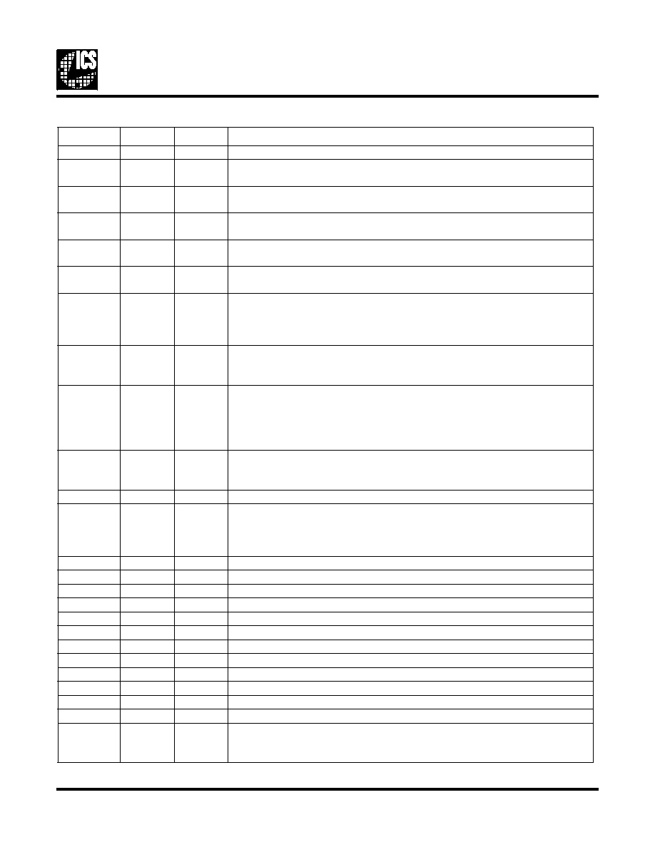
ICS5342
GENDAC
3
CLK1
11
Output
Memory clock output – used to time video memory
CLK0
8
Output
Video clock output – provides a CMOS level pixel or dot clock frequency to
graphics controller – output frequency is determined by values of PLL registers
CS0
2
Input
Clock select 0 – The status of CS0-1 determines which frequency is selected on
the CLK0 (video) output.
CS1
3
Input
Clock select 1– status of CS0-1 determines which frequency is selected on CLK0
(video) output
VREF
46
I/O
Internal reference voltage – normally connects to a 0.1
f capacitor to ground – to
use external Vref, connect 1.235V reference to this pin
RSET
42
Input
Resistor set – pin used to set current level in analog outputs – usually connected
through 1/4W, 1% resistor to ground
SENSE*
68
Output
Monitor sense – Pin is active low when any of red, green, or blue outputs >385mV.
Sense output is high when all analog outputs are < 275 mV. Chip has on-board
comparators and internal 1.235 V voltage reference. This signal is used to detect
monitor type.
BLUE
GREEN
RED
40
38
37
Output
Color signals from DAC analog outputs – Each DAC comprises several current
sources of which outputs are added together according to the applied binary value.
The outputs are typically used to drive a CRT monitor.
P15- P0
13,12,4,1
,
67-64,
58-51
Input
Pixel address lines – Byte-wide information is latched by the rising edge of PCLK
when using the color palette, and is masked by the Pixel Mask register. Values are
used to specify the RAM word address in default mode (accessing RAM). In Hi-
Color XGA, and True Color modes, they represent color data for the DACs.
Ground inputs if they are not used.
PCLK
59
Input
Pixel Clock – rising edge of PCLK controls latching of the Pixel Address and
BLANK* inputs – clock also controls progress of these values through the three-
stage pipeline of the Color Palette RAM, DAC, and outputs
STROBE*
6
Input
latches input clock select signals CS0-CS1
BLANK*
7
Input
Composite BLANK* Signal, active low. When BLANK* is asserted, outputs of
DACs are zero which blacks screen. DACs are automatically powered down to
save current during blanking. Color palette may still be updated through D0-D7
during blanking.
CVDD
9
-
CLK1 Power Supply – connect to DVDD
CVDD
27
-
CLK0 power supply – connect to AVDD
AVDD
41
-
DAC power supply – Connect to AVDD
DVDD
43
-
Digital power supply
XVDD
50
-
Crystal oscillator power supply– connect to AVDD
CVDD
61
-
CLK power supply – connect to DVDD
CGND
10
-
VSS for CLK1 – connect to ground.
CGND
26
-
VSS for CLK0 – connect to ground
XGND
47
-
VSS for crystal oscillator
AGND
36
-
DAC ground – connect to ground
DGND
44
-
Digital ground – connect to ground
CGND
60
-
VSS for CLK – connect to ground
N/C
28-35,
39,45,
62
-
Not connected – leave oating or tie to ground
Pin Description (68-pin PLCC)
Symbol
Pin #
Type
Description
相关PDF资料 |
PDF描述 |
|---|---|
| ICS5342-3 | Analog IC |
| ICS9111M-06 | Miscellaneous Clock Generator |
| ICS9117M02 | Peripheral IC |
| ICS9118M-02 | Miscellaneous Clock Generator |
| ICS9118M-04 | Miscellaneous Clock Generator |
相关代理商/技术参数 |
参数描述 |
|---|---|
| ICS5342-3 | 制造商:ICS 制造商全称:ICS 功能描述:Analog IC |
| ICS5342ADD | 制造商:ICS 制造商全称:ICS 功能描述:Addendum to ICS5342 Data Sheet |
| ICS5342V | 制造商:未知厂家 制造商全称:未知厂家 功能描述:Peripheral IC |
| ICS541 | 制造商:ICS 制造商全称:ICS 功能描述:PRELIMINARY INFORMATION PLL Clock Divider |
| ICS541M | 制造商:ICS 制造商全称:ICS 功能描述:PRELIMINARY INFORMATION PLL Clock Divider |
发布紧急采购,3分钟左右您将得到回复。