- 您现在的位置:买卖IC网 > PDF目录175707 > ICS5342-2 Analog IC PDF资料下载
参数资料
| 型号: | ICS5342-2 |
| 英文描述: | Analog IC |
| 中文描述: | 模拟IC |
| 文件页数: | 35/36页 |
| 文件大小: | 1017K |
| 代理商: | ICS5342-2 |
第1页第2页第3页第4页第5页第6页第7页第8页第9页第10页第11页第12页第13页第14页第15页第16页第17页第18页第19页第20页第21页第22页第23页第24页第25页第26页第27页第28页第29页第30页第31页第32页第33页第34页当前第35页第36页
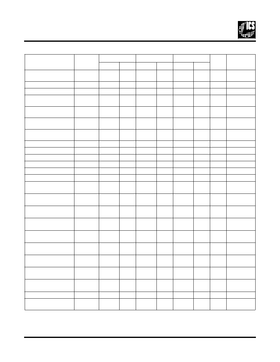
ICS5342
GENDAC
8
Differential output
delay
t
CHAV
2
ns
note G
WR* pulse width low
tWLWH
50
ns
RD* pulse width low
tRLRH
50
ns
Register select setup
time
tSVWL
10
ns
write cycle
Register select setup
time
tSVRL
10
ns
read cycle
Register select hold
time
tWLSX
10
ns
write cycle
Register select hold
time
tRLSX
10
ns
read cycle
WR* data setup time
tDVWH
10
ns
WR* data hold time
tWHDX
10
ns
Output turn-on delay
tRLQX
555ns
RD* enable access time
tRLQV
40
ns
Output hold time
tRHQX
333ns
Output turn-off delay
tRHQZ
20
ns
note H
Successive write inter-
val
tWHWL1
4
(tCHCH)
4
(tCHCH)
4
(tCHCH)
cycle
note I
WR* followed by read
interval
tWHRL1
4
(tCHCH)
4
(tCHCH)
4
(tCHCH)
cycle
note I
Successive read interval
tRHRL1
4
(tCHCH)
4
(tCHCH)
4
(tCHCH)
cycle
note I
RD* followed by write
interval
tRHWL1
4
(tCHCH)
4
(tCHCH)
4
(tCHCH)
cycle
note I
WR* after color write
tWHWL2
4
(tCHCH)
4
(tCHCH)
4
(tCHCH)
cycle
note I
RD* after color write
tWHRL2
4
(tCHCH)
4
(tCHCH)
4
(tCHCH)
cycle
note I
RD* after color read
tRHRL2
8
(tCHCH)
8
(tCHCH)
8
(tCHCH)
cycle
note I
WR* after color read
tRHWL2
8
(tCHCH)
8
(tCHCH)
8
(tCHCH)
cycle
note I
RD* after read address
write
tWHRL3
8
(tCHCH)
8
(tCHCH)
8
(tCHCH)
cycle
note I
SENSE* output delay
tSOD
11
1
s
XIN input clock rise
time
tXCLKR*
15
ns
TTL levels
AC Electrical Characteristics (note: J)
Parameter
Symbol
80 MHZ
110MHz
135Mhz
Units
Test
Conditions
Min
Max
Min
Max
Min
Max
相关PDF资料 |
PDF描述 |
|---|---|
| ICS5342-3 | Analog IC |
| ICS9111M-06 | Miscellaneous Clock Generator |
| ICS9117M02 | Peripheral IC |
| ICS9118M-02 | Miscellaneous Clock Generator |
| ICS9118M-04 | Miscellaneous Clock Generator |
相关代理商/技术参数 |
参数描述 |
|---|---|
| ICS5342-3 | 制造商:ICS 制造商全称:ICS 功能描述:Analog IC |
| ICS5342ADD | 制造商:ICS 制造商全称:ICS 功能描述:Addendum to ICS5342 Data Sheet |
| ICS5342V | 制造商:未知厂家 制造商全称:未知厂家 功能描述:Peripheral IC |
| ICS541 | 制造商:ICS 制造商全称:ICS 功能描述:PRELIMINARY INFORMATION PLL Clock Divider |
| ICS541M | 制造商:ICS 制造商全称:ICS 功能描述:PRELIMINARY INFORMATION PLL Clock Divider |
发布紧急采购,3分钟左右您将得到回复。