- 您现在的位置:买卖IC网 > PDF目录1997 > ICS813078BYILF (IDT, Integrated Device Technology Inc)IC VCXO PLL WIRELESS 64TQFP PDF资料下载
参数资料
| 型号: | ICS813078BYILF |
| 厂商: | IDT, Integrated Device Technology Inc |
| 文件页数: | 1/26页 |
| 文件大小: | 0K |
| 描述: | IC VCXO PLL WIRELESS 64TQFP |
| 标准包装: | 160 |
| 系列: | HiPerClockS™, FemtoClock™ |
| 类型: | 时钟/频率发生器,扇出缓冲器(分配),抖动衰减器,多路复用器 |
| PLL: | 是 |
| 主要目的: | 无线基础架构应用 |
| 输入: | LVDS,LVHSTL,LVPECL,晶体 |
| 输出: | LVPECL |
| 电路数: | 1 |
| 比率 - 输入:输出: | 3:9 |
| 差分 - 输入:输出: | 是/是 |
| 频率 - 最大: | 614.4MHz |
| 电源电压: | 3.135 V ~ 3.465 V |
| 工作温度: | -40°C ~ 85°C |
| 安装类型: | 表面贴装 |
| 封装/外壳: | 64-TQFP 裸露焊盘 |
| 供应商设备封装: | 64-TQFP-EP(10x10) |
| 包装: | 托盘 |
FEMTOCLOCKS VCXO-PLL FREQUENCY GENERATOR
FOR WIRELESS INFRASTRUCTURE EQUIPMENT
ICS813078I
FEMTOCLOCKS VCXO-PLL FREQUENCY GENERATOR
1
ICS813078BYI REV. A OCTOBER 6, 2008
General Description
The ICS813078I is a member of the HiperClocks
family of high performance clock solutions from IDT.
The ICS813078I a PLL based synchronous clock
solution that is optimized for wireless infrastructure
equipment where frequency translation and jitter
attenuation is needed.
The device contains two internal PLL stages that are cascaded in
series. The first PLL stage attenuates the reference clock jitter by
using an internal or external VCXO circuit. The internal VCXO
requires the connection of an external inexpensive pullable crystal
(XTAL) to the ICS813078I. This first PLL stage (VCXO PLL) uses
external passive loop filter components which are used to optimize
the PLL loop bandwidth and damping characteristics for the given
application. The output of the first stage VCXO PLL is a stable and
jitter-tolerant 30.72MHz reference input for the second PLL stage.
The second PLL stage provides frequency translation by
multiplying the output of the first stage up to 491.52MHz or
614.4MHz. The low phase noise characteristics of the VCXO-PLL
clock signal is maintained by the internal FemtoClockPLL, which
requires no external components or complex programming. Two
independently configurable frequency dividers translate the
internal VCO signal to the desired output frequencies. All
frequency translation ratios are set by device configuration pins.
Supported input reference clock frequencies:
10MHz, 12.8MHz, 15MHz, 15.36MHz, 20MHz, 30.72MHz,
61.44MHz, and 122.88MHz
Supported output clock frequencies:
30.72MHz, 38.4MHz, 61.44MHz, 76.8MHz, 122.88MHz,
153.6MHz, 245.76MHz, 491.52MHz, and 614.4MHz
Features
Nine outputs, organized in three independent output banks with
differential LVPECL and single-ended outputs
One differential input clock can accept the following differential
input levels: LVDS, LVPECL, LVHSTL
One single-ended clock input
Frequency generation optimized for wireless infrastructure
Attenuates the phase jitter of the input clock signal by using
low-cost pullable fundamental mode crystal (XTAL)
Internal Femtoclock frequency multiplier stage eliminates the
need for an expensive external high frequency VCXO
LVCMOS levels for all control I/O
RMS phase jitter @ 122.88MHz, using a 30.72MHz crystal
(12kHz to 20MHz): 1.1ps rms (typical)
RMS phase jitter @ 61.44MHz, using a 30.72MHz crystal
(12kHz to 20MHz): 0.97ps rms (typical)
VCXO PLL bandwidth can be optimized for jitter attenuation and
reference frequency tracking using external loop filter
components
PLL fast-lock control
PLL lock detect output
Absolute pull range is +/-50 ppm
Full 3.3V supply voltage
-40°C to 85°C ambient operating temperature
Available in lead-free (RoHS 6) package
HiPerClockS
ICS
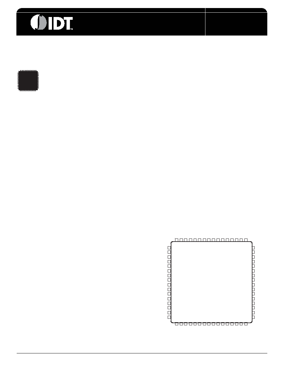
Pin Assignment
64 63 62 61 60 59 58 57 56 55 54 53 52 51 50 49
17 18 19 20 21 22 23 24 25 26 27 28 29 30 31 32
1
2
3
4
5
6
7
8
9
10
11
12
13
14
15
16
48
47
46
45
44
43
42
41
40
39
38
37
36
35
34
33
LF1
LF0
ISET
FLM
VCC
CLK1
nc
NB1
nMR
REF_SEL
CLK0
nCLK0
VEE
NA1
NA0
VCCO
nQA0
QA0
nc
VEE
nc
nQA1
QA1
VCCO
nQA2
QA2
VCC
VEE
nQB0
QB0
NB0
QB1
nSTOPB
NC1
NC0
R2
R1
R0
BYPASS1
BYPASS0
nc
nQ
B
1
nc
V
CCA
n
STOPA
n
STOPC
XTAL__IN
XTAL_OU
T
V
CC
MF
LOCK
V
EE
QC0
V
CCO_CMOS
nc
QC1
V
EE
QC2
V
CCO_CMOS
V
EE
QC3
V
EE
64-Lead TQFP, E-Pad
10mm x 10mm x 1mm
package body
Y Package
相关PDF资料 |
PDF描述 |
|---|---|
| ICS813323BGLF | IC ATTENUATOR/MULTIPLIER 24TSSOP |
| ICS840002AGLF | IC FREQ SYNTHESIZER 16-TSSOP |
| ICS840022AKI-02LF | IC CLOCK GENERATOR 16VFQFPN |
| ICS84021AYLF | IC SYNTHESIZER HIGH FREQ 32-LQFP |
| ICS840245AGILF | IC FREQ SYNTHESIZER 16-TSSOP |
相关代理商/技术参数 |
参数描述 |
|---|---|
| ICS813078BYILFT | 功能描述:IC VCXO PLL WIRELESS 64TQFP RoHS:是 类别:集成电路 (IC) >> 时钟/计时 - 专用 系列:HiPerClockS™, FemtoClock™ 标准包装:1,500 系列:- 类型:时钟缓冲器/驱动器 PLL:是 主要目的:- 输入:- 输出:- 电路数:- 比率 - 输入:输出:- 差分 - 输入:输出:- 频率 - 最大:- 电源电压:3.3V 工作温度:0°C ~ 70°C 安装类型:表面贴装 封装/外壳:28-SSOP(0.209",5.30mm 宽) 供应商设备封装:28-SSOP 包装:带卷 (TR) 其它名称:93786AFT |
| ICS813078I | 制造商:IDT 制造商全称:Integrated Device Technology 功能描述:FEMTOCLOCKS? VCXO-PLL FREQUENCY GENERATOR FOR WIRELESS INFRASTRUCTURE EQUIPMENT |
| ICS813252CKI-02LF | 功能描述:IC MULTIPLIER VCXO PLL 32-VFQFPN RoHS:是 类别:集成电路 (IC) >> 时钟/计时 - 时钟发生器,PLL,频率合成器 系列:HiPerClockS™, FemtoClock™ 标准包装:27 系列:Precision Edge® 类型:频率合成器 PLL:是 输入:PECL,晶体 输出:PECL 电路数:1 比率 - 输入:输出:1:1 差分 - 输入:输出:无/是 频率 - 最大:800MHz 除法器/乘法器:是/无 电源电压:3.135 V ~ 5.25 V 工作温度:0°C ~ 85°C 安装类型:表面贴装 封装/外壳:28-SOIC(0.295",7.50mm 宽) 供应商设备封装:28-SOIC 包装:管件 |
| ICS813252CKI-02LFT | 功能描述:IC MULTIPLIER VCXO PLL 32-VFQFPN RoHS:是 类别:集成电路 (IC) >> 时钟/计时 - 时钟发生器,PLL,频率合成器 系列:HiPerClockS™, FemtoClock™ 标准包装:27 系列:Precision Edge® 类型:频率合成器 PLL:是 输入:PECL,晶体 输出:PECL 电路数:1 比率 - 输入:输出:1:1 差分 - 输入:输出:无/是 频率 - 最大:800MHz 除法器/乘法器:是/无 电源电压:3.135 V ~ 5.25 V 工作温度:0°C ~ 85°C 安装类型:表面贴装 封装/外壳:28-SOIC(0.295",7.50mm 宽) 供应商设备封装:28-SOIC 包装:管件 |
| ICS813252I-02 | 制造商:IDT 制造商全称:Integrated Device Technology 功能描述:VCXO JITTER ATTENUATOR & FEMTOCLOCK? MULTIPLIER |
发布紧急采购,3分钟左右您将得到回复。