- 您现在的位置:买卖IC网 > PDF目录67710 > ICSSSTUA32S865AHLF-T (INTEGRATED DEVICE TECHNOLOGY INC) SSTU SERIES, POSITIVE EDGE TRIGGERED D FLIP-FLOP, TRUE OUTPUT, PBGA160 PDF资料下载
参数资料
| 型号: | ICSSSTUA32S865AHLF-T |
| 厂商: | INTEGRATED DEVICE TECHNOLOGY INC |
| 元件分类: | 锁存器 |
| 英文描述: | SSTU SERIES, POSITIVE EDGE TRIGGERED D FLIP-FLOP, TRUE OUTPUT, PBGA160 |
| 封装: | 9 X 13 MM, LEAD FREE, BGA-160 |
| 文件页数: | 12/17页 |
| 文件大小: | 199K |
| 代理商: | ICSSSTUA32S865AHLF-T |
4
ICSSSTUA32S865A
1053A—03/21/05
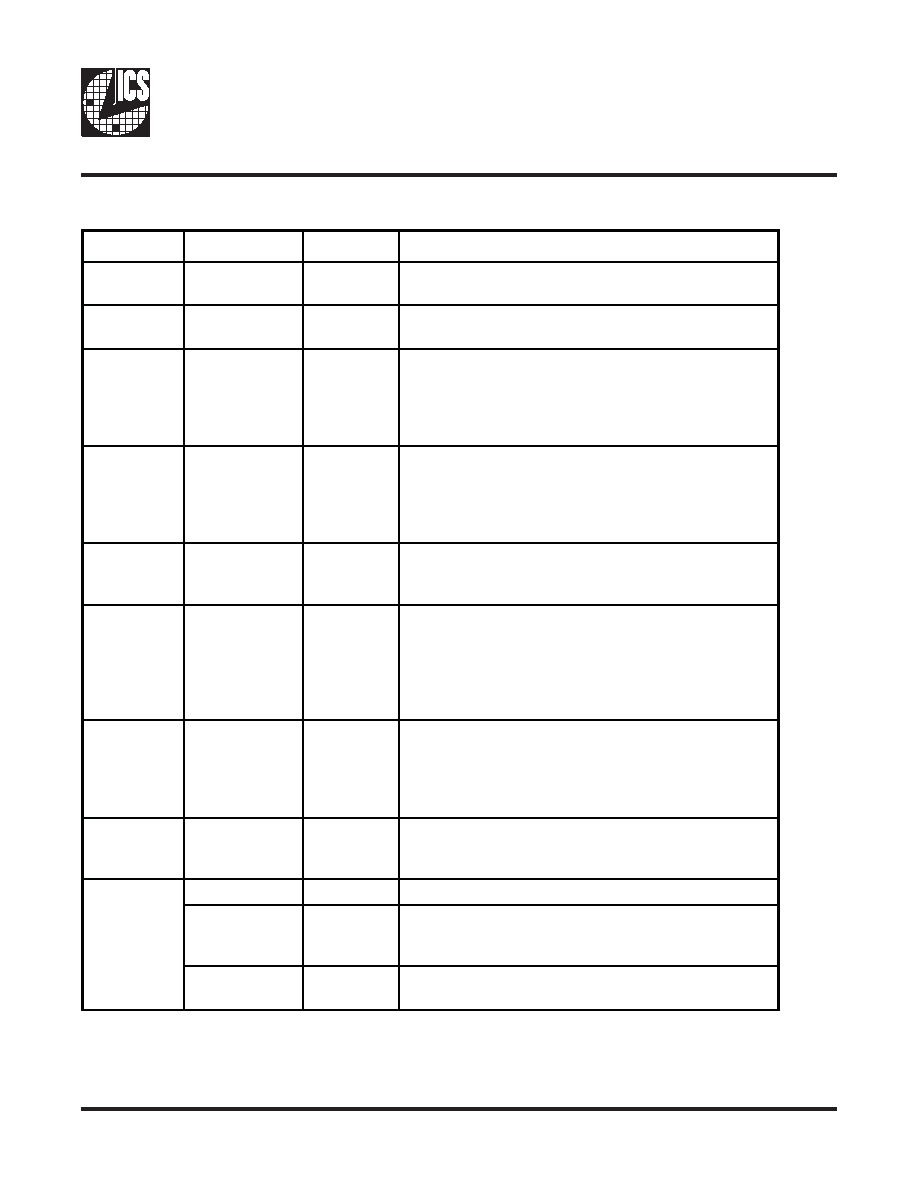
Ball Assignment
Signal Group
Signal Name
Type
Description
Ungated inputs DCKE0, DCKE1,
DODT0, DODT1
SSTL_18
DRAM function pins not associated with Chip Select.
Chip Select
gated inputs
D0 ... D21
SSTL_18
DRAM inputs, re-driven only when Chip Select is LOW.
Chip Select
inputs
DCS0# , DCS1#
SSTL_18
DRAM Chip Select signals. These pins initiate DRAM
address/command decodes, and as such at least one will be
low when a valid address/command is present. The register
can be programmed to re-drive all D-inputs only (CSGateEN
high) when at least one Chip Select input is LOW.
Re-driven
outputs
Q0A...Q21A,
Q0B ... Q21B,
QCS#0-1A,B,
QCKE0-1A,B,
QODT0-1A,B
SSTL_18
Outputs of the register, valid after the specified clock count
and immediately following a rising edge of the clock.
Parity input
PARIN
SSTL_18
Input parity is received on pin PARIN and should maintain
odd parity across the D0...D21 inputs, at the rising edge of the
clock.
Parity error
output
PTYERR#
Open drain
When LOW, this output indicates that a parity error was
identified associated with the address and/or command inputs.
PTYERR# will be active for two clock cycles, and delayed by
an additional clock cycle for compatibility with final parity
out timing on the industry-standard DDR-II register with
parity (in JEDEC definition).
Program inputs CSGateEN
1.8 V
LVCMOS
Chip Select Gate Enable. When HIGH, the D0..D21 inputs
will be latched only when at least one Chip Select input is
LOW during the rising edge of the clock. When LOW, the
D0...D21 inputs will be latched and redriven on every rising
edge of the clock.
Clock inputs
CK, CK#
SSTL_18
Differential master clock input pair to the register. The
register operation is triggered by a rising edge on the positive
clock input (CK).
Miscellaneous
inputs
MCL, MCH
Must be connectedd to a logic LOW or HIGH.
RESET#
1.8 V
LVCMOS
Asynchronous reset input. When LOW, it causes a reset of the
internal latches, thereby forcing the outputs LOW. RESET#
also resets the PTYERR# signal.
VREF
0.9 V nominal Input reference voltage for the SSTL_18 inputs. Two pins
(internally tied together) are used for increased reliability.
相关PDF资料 |
PDF描述 |
|---|---|
| ICSSSTUB32871AHMLFT | 32871 SERIES, POSITIVE EDGE TRIGGERED D FLIP-FLOP, TRUE OUTPUT, PBGA96 |
| ICSSSTUF32864AYH-T | SSTU SERIES, POSITIVE EDGE TRIGGERED D FLIP-FLOP, TRUE OUTPUT, PBGA96 |
| ICSSSTUF32864AYHLF-T | SSTU SERIES, POSITIVE EDGE TRIGGERED D FLIP-FLOP, TRUE OUTPUT, PBGA96 |
| ICSSSTUF32864AYHLF-T | SSTU SERIES, POSITIVE EDGE TRIGGERED D FLIP-FLOP, TRUE OUTPUT, PBGA96 |
| ICSSSTUF32864YHLFT | SSTU SERIES, POSITIVE EDGE TRIGGERED D FLIP-FLOP, TRUE OUTPUT, PBGA96 |
相关代理商/技术参数 |
参数描述 |
|---|---|
| ICSSSTUA32S869B | 制造商:ICS 制造商全称:ICS 功能描述:14-Bit Configurable Registered Buffer for DDR2 |
| ICSSSTUAF32865A | 制造商:IDT 制造商全称:Integrated Device Technology 功能描述:25-BIT CONFIGURABLE REGISTERED BUFFER FOR DDR2 |
| ICSSSTUAF32865AHLFT | 制造商:IDT 制造商全称:Integrated Device Technology 功能描述:25-BIT CONFIGURABLE REGISTERED BUFFER FOR DDR2 |
| ICSSSTUAF32866B | 制造商:IDT 制造商全称:Integrated Device Technology 功能描述:25-BIT CONFIGURABLE REGISTERED BUFFER FOR DDR2 |
| ICSSSTUAF32866BHLFT | 制造商:IDT 制造商全称:Integrated Device Technology 功能描述:25-BIT CONFIGURABLE REGISTERED BUFFER FOR DDR2 |
发布紧急采购,3分钟左右您将得到回复。