- 您现在的位置:买卖IC网 > PDF目录10031 > IDT72V3612L15PF8 (IDT, Integrated Device Technology Inc)IC FIFO 64X36X2 15NS 120QFP PDF资料下载
参数资料
| 型号: | IDT72V3612L15PF8 |
| 厂商: | IDT, Integrated Device Technology Inc |
| 文件页数: | 24/24页 |
| 文件大小: | 0K |
| 描述: | IC FIFO 64X36X2 15NS 120QFP |
| 标准包装: | 750 |
| 系列: | 72V |
| 功能: | 异步 |
| 存储容量: | 4.6K(64 x 36 x2) |
| 数据速率: | 67MHz |
| 访问时间: | 15ns |
| 电源电压: | 3 V ~ 3.6 V |
| 工作温度: | 0°C ~ 70°C |
| 安装类型: | 表面贴装 |
| 封装/外壳: | 120-LQFP |
| 供应商设备封装: | 120-TQFP(14x14) |
| 包装: | 带卷 (TR) |
| 其它名称: | 72V3612L15PF8 |
9
IDT72V3612 3.3V, CMOS SyncBiFIFOTM
64 x 36 x 2
COMMERCIALTEMPERATURERANGE
SIGNAL DESCRIPTIONS
RESET
The IDT72V3612 is reset by taking the Reset (RST) input LOW for at
least four port A Clock (CLKA) and four port B Clock (CLKB) LOW-to-HIGH
transitions. The Reset input can switch asynchronously to the clocks. A
device reset initializes the internal read and write pointers of each FIFO and
forces the Full Flags (FFA, FFB) LOW, the Empty Flags (EFA, EFB) LOW,
the Almost-Empty flags (AEA, AEB) LOW and the Almost-Full flags (AFA,
AFB) HIGH. A reset also forces the Mailbox Flags (MBF1, MBF2) HIGH.
After a reset, FFA is set HIGH after two LOW-to-HIGH transitions of CLKA
and FFB is set HIGH after two LOW-to-HIGH transitions of CLKB. The
device must be reset after power up before data is written to its memory.
A LOW-to-HIGH transition on the RST input loads the Almost-Full and
Almost-Emptyregisters(X)withthevaluesselectedbytheFlagSelect(FS0,
FS1) inputs. The values that can be loaded into the registers are shown in
Table 1.FortherelevantResetandpresetvalueloadingtimingdiagram,see
Figure 2.
FIFO WRITE/READ OPERATION
The state of port A data A0-A35 outputs is controlled by the port A Chip
Select (CSA) and the port A Write/Read select (W/RA). The A0-A35 outputs
are in the high-impedance state when either CSA or W/RA is HIGH. The A0-
A35 outputs are active when both CSA and W/RA are LOW.
Data is loaded into FIFO1 from the A0-A35 inputs on a LOW-to-HIGH
transition of CLKA when CSA is LOW, W/RA is HIGH, ENA is HIGH, MBA
is LOW, and FFA is HIGH. Data is read from FIFO2 to the A0-A35 outputs
by a LOW-to-HIGH transition of CLKA when CSA is LOW, W/RA is LOW,
ENA is HIGH, MBA is LOW, and EFA is HIGH (see Table 2). Relevant Write
and Read timing diagrams for Port A can be found in Figure 3 and Figure
6.
The port B control signals are identical to those of port A. The state of
the port B data (B0-B35) outputs is controlled by the port B Chip Select
(CSB) and the port B Write/Read select (W/RB). The B0-B35 outputs are
in the high-impedance state when either CSB or W/RB is HIGH. The B0-
B35 outputs are active when both CSB and W/RB are LOW.
Data is loaded into FIFO2 from the B0-B35 inputs on a LOW-to-HIGH
transition of CLKB when CSB is LOW, W/RB is HIGH, ENB is HIGH, MBB
is LOW, and FFB is HIGH. Data is read from FIFO1 to the B0-B35 outputs
byaLOW-to-HIGHtransitionofCLKBwhenCSBisLOW,W/RBisLOW,ENB
is HIGH, MBB is LOW, and EFB is HIGH (see Table 3). Relevant Write and
Read timing diagrams for Port B can be found in Figure 4 and Figure 5.
ThesetupandholdtimeconstraintstotheportclocksfortheportChipSelects
(CSA,CSB)andWrite/Readselects(W/RA,W/RB)areonlyforenablingwrite
CSB
W/RB
ENB
MBB
CLKB
Data B (B0-B35) I/O
Port Functions
H
X
Input
None
L
H
L
X
Input
None
LH
H
L
↑
Input
FIFO2 Write
LH
H
↑
Input
Mail2 Write
L
X
Output
None
LL
H
L
↑
Output
FIFO1 read
L
H
X
Output
None
LL
H
↑
Output
Mail1 Read (Set MBF1 HIGH)
CSA
W/RA
ENA
MBA
CLKA
Data A (A0-A35) I/O
Port Functions
H
X
Input
None
L
H
L
X
Input
None
LH
H
L
↑
Input
FIFO1 Write
LH
H
↑
Input
Mail1 Write
L
X
Output
None
LL
H
L
↑
Output
FIFO2 Read
L
H
X
Output
None
LL
H
↑
Output
Mail2 Read (Set MBF2 HIGH)
ALMOST-FULL AND
FS1
FS0
RST
ALMOST-EMPTY FLAG
OFFSET REGISTER (X)
HH
↑
16
HL
↑
12
LH
↑
8
LL
↑
4
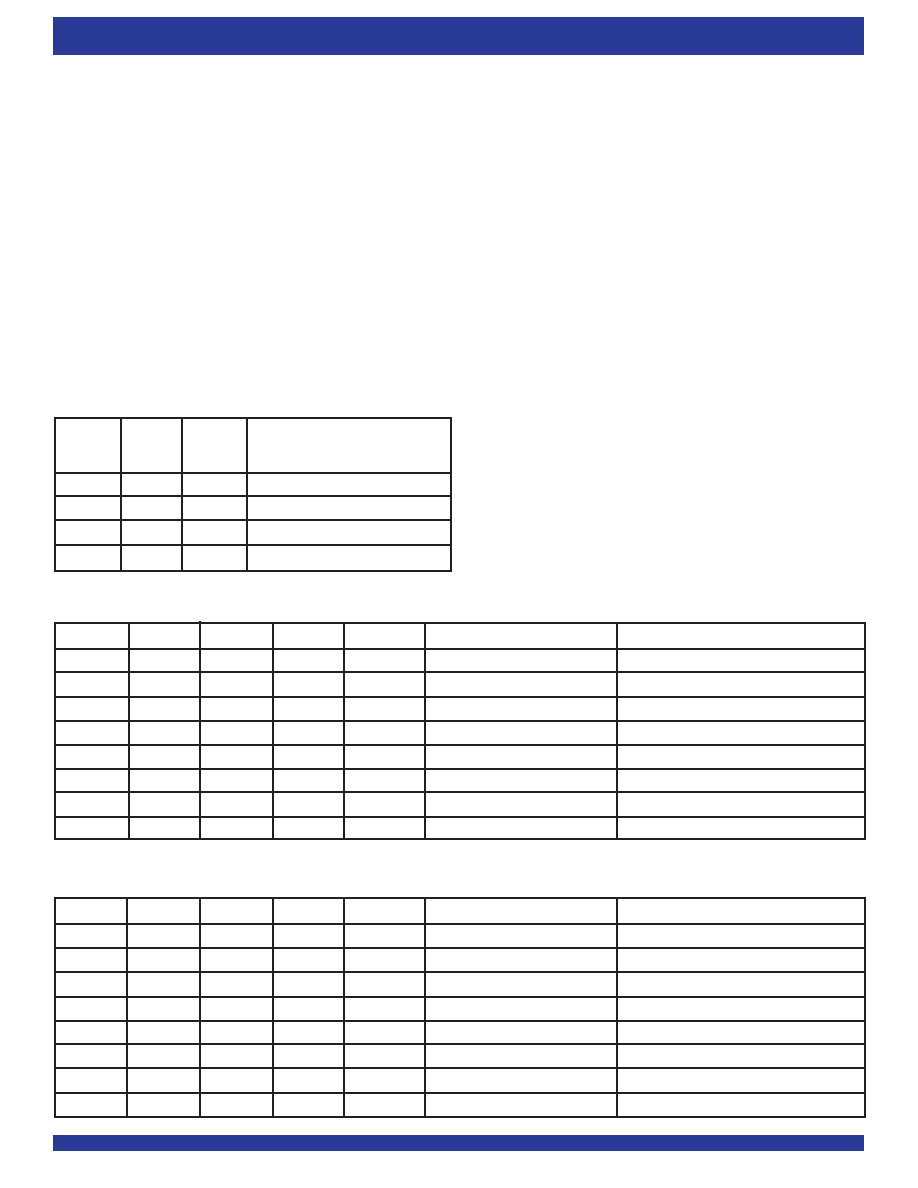
TABLE 1 – FLAG PROGRAMMING
TABLE 2 – PORT-A ENABLE FUNCTION TABLE
TABLE 3 – PORT-B ENABLE FUNCTION TABLE
相关PDF资料 |
PDF描述 |
|---|---|
| AD678BD | IC ADC 12BIT SAMPLING 28-CDIP |
| AD1555BPZRL | IC ADC PGA 24BIT LN 28-PLCC |
| VI-26M-MX-F1 | CONVERTER MOD DC/DC 10V 75W |
| AD678AJ | IC ADC 12BIT 200KSPS 44-JLCC |
| IDT72V3611L15PF8 | IC FIFO SYNC 64X36 15NS 120-TQFP |
相关代理商/技术参数 |
参数描述 |
|---|---|
| IDT72V3612L15PQF | 功能描述:IC FIFO 64X36X2 15NS 132QFP RoHS:否 类别:集成电路 (IC) >> 逻辑 - FIFO 系列:72V 标准包装:90 系列:7200 功能:同步 存储容量:288K(16K x 18) 数据速率:100MHz 访问时间:10ns 电源电压:4.5 V ~ 5.5 V 工作温度:0°C ~ 70°C 安装类型:表面贴装 封装/外壳:64-LQFP 供应商设备封装:64-TQFP(14x14) 包装:托盘 其它名称:72271LA10PF |
| IDT72V3612L20PF | 功能描述:IC FIFO 64X36X2 20NS 120QFP RoHS:否 类别:集成电路 (IC) >> 逻辑 - FIFO 系列:72V 标准包装:90 系列:7200 功能:同步 存储容量:288K(16K x 18) 数据速率:100MHz 访问时间:10ns 电源电压:4.5 V ~ 5.5 V 工作温度:0°C ~ 70°C 安装类型:表面贴装 封装/外壳:64-LQFP 供应商设备封装:64-TQFP(14x14) 包装:托盘 其它名称:72271LA10PF |
| IDT72V3612L20PF8 | 功能描述:IC FIFO 64X36X2 20NS 120QFP RoHS:否 类别:集成电路 (IC) >> 逻辑 - FIFO 系列:72V 标准包装:90 系列:7200 功能:同步 存储容量:288K(16K x 18) 数据速率:100MHz 访问时间:10ns 电源电压:4.5 V ~ 5.5 V 工作温度:0°C ~ 70°C 安装类型:表面贴装 封装/外壳:64-LQFP 供应商设备封装:64-TQFP(14x14) 包装:托盘 其它名称:72271LA10PF |
| IDT72V3612L20PQF | 功能描述:IC FIFO 64X36X2 20NS 132QFP RoHS:否 类别:集成电路 (IC) >> 逻辑 - FIFO 系列:72V 标准包装:90 系列:7200 功能:同步 存储容量:288K(16K x 18) 数据速率:100MHz 访问时间:10ns 电源电压:4.5 V ~ 5.5 V 工作温度:0°C ~ 70°C 安装类型:表面贴装 封装/外壳:64-LQFP 供应商设备封装:64-TQFP(14x14) 包装:托盘 其它名称:72271LA10PF |
| IDT72V3613L12PF | 功能描述:IC FIFO CLOCK 64X36 12NS 120TQFP RoHS:否 类别:集成电路 (IC) >> 逻辑 - FIFO 系列:72V 标准包装:90 系列:7200 功能:同步 存储容量:288K(16K x 18) 数据速率:100MHz 访问时间:10ns 电源电压:4.5 V ~ 5.5 V 工作温度:0°C ~ 70°C 安装类型:表面贴装 封装/外壳:64-LQFP 供应商设备封装:64-TQFP(14x14) 包装:托盘 其它名称:72271LA10PF |
发布紧急采购,3分钟左右您将得到回复。