- 您现在的位置:买卖IC网 > PDF目录10015 > IDT72V3622L10PF8 (IDT, Integrated Device Technology Inc)IC BIFIFO 256X36X2 10NS 120-TQFP PDF资料下载
参数资料
| 型号: | IDT72V3622L10PF8 |
| 厂商: | IDT, Integrated Device Technology Inc |
| 文件页数: | 3/29页 |
| 文件大小: | 0K |
| 描述: | IC BIFIFO 256X36X2 10NS 120-TQFP |
| 标准包装: | 750 |
| 系列: | 72V |
| 功能: | 异步,同步 |
| 存储容量: | 18.4K(256 x 36 x 2) |
| 数据速率: | 100MHz |
| 访问时间: | 10ns |
| 电源电压: | 3 V ~ 3.6 V |
| 工作温度: | 0°C ~ 70°C |
| 安装类型: | 表面贴装 |
| 封装/外壳: | 120-LQFP |
| 供应商设备封装: | 120-TQFP(14x14) |
| 包装: | 带卷 (TR) |
| 其它名称: | 72V3622L10PF8 |
第1页第2页当前第3页第4页第5页第6页第7页第8页第9页第10页第11页第12页第13页第14页第15页第16页第17页第18页第19页第20页第21页第22页第23页第24页第25页第26页第27页第28页第29页
11
COMMERCIAL TEMPERATURERANGE
IDT72V3622/72V3632/72V3642 CMOS 3.3V SyncBiFIFOTM
256 x 36 x 2, 512 x 36 x 2, 1,024 x 36 x 2
FIFO WRITE/READ OPERATION
ThestateoftheportAdata(A0-A35)outputsiscontrolledbyportAChip
Select (CSA) and port A Write/Read select (W/RA). The A0-A35 outputs are
in the high-impedance state when either CSA or W/RA is HIGH. The A0-A35
outputs are active when both CSA and W/RA are LOW.
Data is loaded into FIFO1 from the A0-A35 inputs on a LOW-to-HIGH
transition of CLKA when CSA is LOW, W/RA is HIGH, ENA is HIGH , MBA is
LOW, and FFA/IRA is HIGH. Data is read from FIFO2 to the A0-A35 outputs
byaLOW-to-HIGHtransitionofCLKAwhenCSAisLOW,W/RAisLOW,ENA
isHIGH,MBAisLOW,andEFA/ORAisHIGH(seeTable2).FIFOreadsand
writesonportAareindependentofanyconcurrentportBoperation.Writeand
Read cycle timing diagrams for Port A can be found in Figure 4 and 7.
TheportBcontrolsignalsareidenticaltothoseofportAwiththeexception
thattheportBWrite/Readselect(W/RB)istheinverseoftheportAWrite/Read
select(W/RA).ThestateoftheportBdata(B0-B35)outputsiscontrolledbythe
port B Chip Select (CSB) and port B Write/Read select (W/RB). The B0-B35
outputs are in the high-impedance state when either CSB is HIGH or W/RB
isLOW.TheB0-B35outputsareactivewhenCSBisLOWandW/RBisHIGH.
Data is loaded into FIFO2 from the B0-B35 inputs on a LOW-to-HIGH
transition of CLKB when CSB is LOW, W/RB is LOW, ENB is HIGH, MBB is
LOW, and FFB/IRB is HIGH. Data is read from FIFO1 to the B0-B35 outputs
byaLOW-to-HIGHtransitionofCLKBwhenCSBisLOW,W/RBisHIGH,ENB
isHIGH,MBBisLOW,andEFB/ORBisHIGH(seeTable3).FIFOreadsand
writesonportBareindependentofanyconcurrentportAoperation.Writeand
Read cycle timing diagrams for Port B can be found in Figure 5 and 6.
The setup and hold time constraints to the port Clocks for the port Chip
SelectsandWrite/Readselectsareonlyforenablingwriteandreadoperations
andarenotrelatedtohigh-impedancecontrolofthedataoutputs.Ifaportenable
isLOWduringaclockcycle,theport’sChipSelectandWrite/Readselectmay
change states during the setup and hold time window of the cycle.
WhenoperatingtheFIFOinFWFTmodeandtheOutputReadyflagisLOW,
thenextwordwrittenisautomaticallysenttotheFIFO’soutputregisterbythe
LOW-to-HIGHtransitionoftheportclockthatsetstheOutputReadyflagHIGH.
WhentheOutputReadyflagisHIGH,subsequentdataisclockedtotheoutput
registersonlywhenareadisselectedusingtheport’sChipSelect,Write/Read
select, Enable, and Mailbox select.
When operating the FIFO in IDT Standard mode, the first word will cause
theEmptyFlagtochangestateonthesecondLOW-to-HIGHtransitionofthe
ReadClock. Thedatawordwillnotbeautomaticallysenttotheoutputregister.
Instead, data residing in the FIFO's memory array is clocked to the output
registeronlywhenareadisselected usingtheport’sChipSelect,Write/Read
select, Enable, and Mailbox select.
SYNCHRONIZED FIFO FLAGS
Each FIFO is synchronized to its port clock through at least two flip-flop
stages.Thisisdonetoimproveflagsignalreliabilitybyreducingtheprobability
of metastable events when CLKA and CLKB operate asynchronously to one
another. EFA/ORA, AEA, FFA/IRA, and AFA are synchronized to CLKA.
EFB/ORB, AEB, FFB/IRB, and AFB
are synchronized to CLKB. Tables
4 and 5 show the relationship of each port flag to FIFO1 and FIFO2.
EMPTY/OUTPUT READY FLAGS (EFA/ORA, EFB/ORB)
These are dual purpose flags. In the FWFT mode, the Output Ready
(ORA, ORB) function is selected. When the Output Ready flag is HIGH,
CSB
W/RB
ENB
MBB
CLKB
Data B (B0-B35) I/O
Port Function
H
X
High-Impedance
None
L
X
Input
None
LL
H
L
↑
Input
FIFO2 write
LL
H
↑
Input
Mail2write
L
H
L
X
Output
None
LH
H
L
↑
Output
FIFO1 read
L
H
L
H
X
Output
None
LH
H
↑
Output
Mail1 read (set MBF1 HIGH)
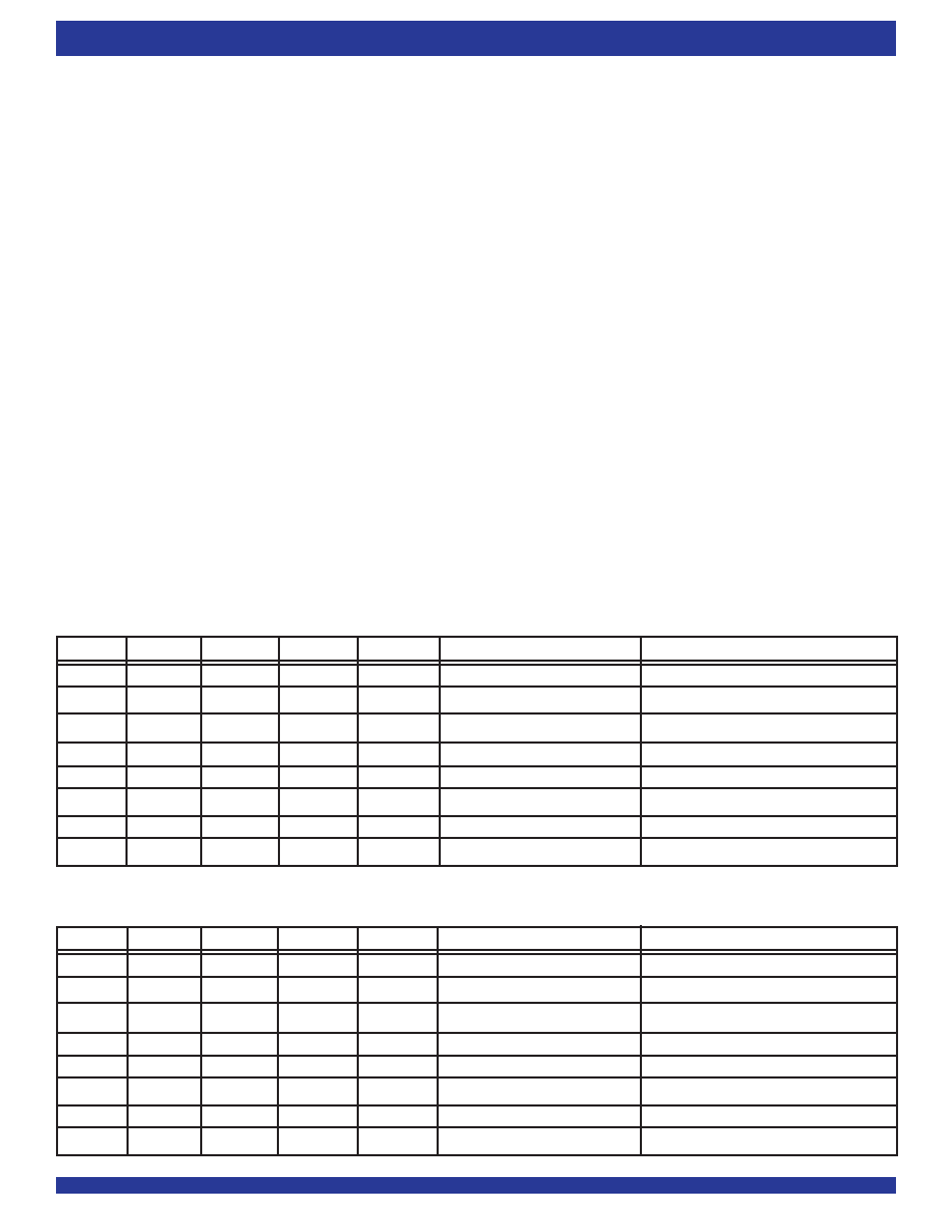
TABLE 3 — PORT B ENABLE FUNCTION TABLE
TABLE 2 — PORT A ENABLE FUNCTION TABLE
CSA
W/RA
ENA
MBA
CLKA
Data A (A0-A35) I/O
Port Function
H
X
High-Impedance
None
L
H
L
X
Input
None
LH
H
L
↑
Input
FIFO1 write
LH
H
↑
Input
Mail1write
L
X
Output
None
LL
H
L
↑
Output
FIFO2 read
L
H
X
Output
None
LL
H
↑
Output
Mail2 read (set MBF2 HIGH)
相关PDF资料 |
PDF描述 |
|---|---|
| MS27467E17B55PD | CONN PLUG 55POS STRAIGHT W/PINS |
| VE-240-IU-F1 | CONVERTER MOD DC/DC 5V 200W |
| VE-B32-MX-B1 | CONVERTER MOD DC/DC 15V 75W |
| VI-21T-MY | CONVERTER MOD DC/DC 6.5V 50W |
| LTC1544IG#TR | IC TXRX SFTWR SEL DTE/DCE 28SSOP |
相关代理商/技术参数 |
参数描述 |
|---|---|
| IDT72V3622L10PFG | 制造商:Integrated Device Technology Inc 功能描述:IC BIFIFO 256X36X2 10NS 120-TQFP |
| IDT72V3622L10PFG8 | 制造商:Integrated Device Technology Inc 功能描述:IC BIFIFO 256X36X2 10NS 120-TQFP |
| IDT72V3622L10PQF | 功能描述:IC BIFIFO 256X36X2 10NS 132-PQFP RoHS:否 类别:集成电路 (IC) >> 逻辑 - FIFO 系列:72V 标准包装:90 系列:7200 功能:同步 存储容量:288K(16K x 18) 数据速率:100MHz 访问时间:10ns 电源电压:4.5 V ~ 5.5 V 工作温度:0°C ~ 70°C 安装类型:表面贴装 封装/外壳:64-LQFP 供应商设备封装:64-TQFP(14x14) 包装:托盘 其它名称:72271LA10PF |
| IDT72V3622L15PF | 功能描述:IC BIFIFO 256X36X2 15NS 120-TQFP RoHS:否 类别:集成电路 (IC) >> 逻辑 - FIFO 系列:72V 标准包装:90 系列:7200 功能:同步 存储容量:288K(16K x 18) 数据速率:100MHz 访问时间:10ns 电源电压:4.5 V ~ 5.5 V 工作温度:0°C ~ 70°C 安装类型:表面贴装 封装/外壳:64-LQFP 供应商设备封装:64-TQFP(14x14) 包装:托盘 其它名称:72271LA10PF |
| IDT72V3622L15PF8 | 功能描述:IC BIFIFO 256X36X2 15NS 120-TQFP RoHS:否 类别:集成电路 (IC) >> 逻辑 - FIFO 系列:72V 标准包装:90 系列:7200 功能:同步 存储容量:288K(16K x 18) 数据速率:100MHz 访问时间:10ns 电源电压:4.5 V ~ 5.5 V 工作温度:0°C ~ 70°C 安装类型:表面贴装 封装/外壳:64-LQFP 供应商设备封装:64-TQFP(14x14) 包装:托盘 其它名称:72271LA10PF |
发布紧急采购,3分钟左右您将得到回复。