- 您现在的位置:买卖IC网 > PDF目录9968 > IDT82V2088BB (IDT, Integrated Device Technology Inc)IC LIU T1/J1/E1 8CH 208-BGA PDF资料下载
参数资料
| 型号: | IDT82V2088BB |
| 厂商: | IDT, Integrated Device Technology Inc |
| 文件页数: | 16/78页 |
| 文件大小: | 0K |
| 描述: | IC LIU T1/J1/E1 8CH 208-BGA |
| 标准包装: | 10 |
| 类型: | 线路接口装置(LIU) |
| 规程: | E1 |
| 电源电压: | 3.13 V ~ 3.47 V |
| 安装类型: | 表面贴装 |
| 封装/外壳: | 208-BGA |
| 供应商设备封装: | 208-PBGA(17x17) |
| 包装: | 托盘 |
| 其它名称: | 82V2088BB |
第1页第2页第3页第4页第5页第6页第7页第8页第9页第10页第11页第12页第13页第14页第15页当前第16页第17页第18页第19页第20页第21页第22页第23页第24页第25页第26页第27页第28页第29页第30页第31页第32页第33页第34页第35页第36页第37页第38页第39页第40页第41页第42页第43页第44页第45页第46页第47页第48页第49页第50页第51页第52页第53页第54页第55页第56页第57页第58页第59页第60页第61页第62页第63页第64页第65页第66页第67页第68页第69页第70页第71页第72页第73页第74页第75页第76页第77页第78页
23
INDUSTRIAL
TEMPERATURE RANGES
OCTAL CHANNEL T1/E1/J1 LONG HAUL/SHORT HAUL LINE INTERFACE UNIT
3.3.2
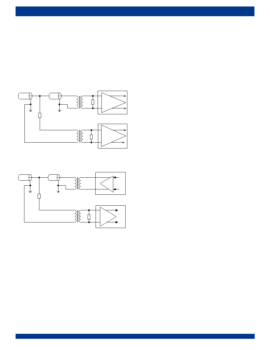
LINE MONITOR
In both T1/J1 and E1 short haul applications, the non-intrusive monitor-
ingonchannelslocatedinotherchipscanbeperformedbytappingthemon-
itored channel through a high impedance bridging circuit. Refer to Figure-
After a high resistance bridging circuit, the signal arriving at the RTIPn/
RRINGn is dramatically attenuated. To compensate this attenuation, the
Monitor Gain can be used to boost the signal by 22 dB, 26 dB and 32 dB,
selected by MG[1:0] bits (RCF2, 09H...). For normal operation, the Monitor
Gain should be set to 0 dB.
Figure-10 Monitoring Receive Line in Another Chip
Figure-11 Monitor Transmit Line in Another Chip
3.3.3
ADAPTIVE EQUALIZER
The adaptive equalizer can remove most of the signal distortion due to
intersymbol interference caused by cable attenuation. It can be enabled or
disabled by setting EQ_ON bit to ‘1’ or ‘0’ (RCF1, 08H...).
When the adaptive equalizer is out of range, EQ_S bit (STAT0, 14H...)
will be set to ‘1’ to indicate the status of equalizer. If EQ_IES bit (INTES,
13H...) is set to ‘1’, any changes of EQ_S bit will generate an interrupt and
EQ_IS bit (INTS0, 16H...) will be set to ‘1’ if it is not masked. If EQ_IES bit
is set to ‘0’, only the ‘0’ to ‘1’ transition of the EQ_S bit will generate an inter-
rupt and EQ_IS bit will be set to ‘1’ if it is not masked. The EQ_IS bit will be
reset after being read.
The Amplitude/wave shape detector keeps on measuring the ampli-
tude/waveshapeoftheincomingsignalsduringanobservationperiod.This
observation period can be 32, 64, 128 or 256 symbol periods, as selected
by UPDW[1:0] bits (RCF2, 09H...). A shorter observation period allows
quicker response to pulse amplitude variation while a longer observation
period can minimize the possible overshoots. The default observation
period is 128 symbol periods.
Based on the observed peak value for a period, the equalizer will be
adjusted to achieve a normalized signal. LATT[4:0] bits (STAT1, 15H...)
indicate the signal attenuation introduced by the cable in approximately 2
dB per step.
3.3.4
RECEIVE SENSITIVITY
For short haul application, the Receive Sensitivity for both E1 and T1/
J1 is -10 dB. For long haul application, the receive sensitivity is -43 dB for
E1 and -36 dB for T1/J1.
3.3.5
DATA SLICER
The Data Slicer is used to generate a standard amplitude mark or a
space according to the amplitude of the input signals. The threshold can
be 40%, 50%, 60% or 70%, as selected by the SLICE[1:0] bits (RCF2,
09H...). The output of the Data Slicer is forwarded to the CDR (Clock & Data
Recovery) unit or to the RDPn/RDNn pins directly if the CDR is disabled.
3.3.6
CDR (Clock & Data Recovery)
The CDR is used to recover the clock from the received signals. The
recovered clock tracks the jitter in the data output from the Data Slicer and
keeps the phase relationship between data and clock during the absence
of the incoming pulse. The CDR can also be by-passed in the Dual Rail
mode. When CDR is by-passed, the data from the Data Slicer is output to
the RDPn/RDNn pins directly.
3.3.7
DECODER
In T1/J1 applications, the R_MD[1:0] bits (RCF0, 07H...) is used to
selecttheAMIdecoderorB8ZSdecoder.InE1applications,theR_MD[1:0]
bits (RCF0, 07H...) are used to select the AMI decoder or HDB3 decoder.
3.3.8
RECEIVE PATH SYSTEM INTERFACE
The receive path system interface consists of RCLKn pin, RDn/RDPn
pin and RDNn pin. In E1 mode, the RCLKn outputs a recovered 2.048 MHz
clock.InT1/J1mode,theRCLKnoutputsarecovered1.544MHzclock.The
received data is updated on the RDn/RDPn and RDNn pins on the active
edge of RCLKn. The active edge of RCLKn can be selected by the
RCLK_SEL bit (RCF0, 07H...). And the active level of the data on RDn/
RDPn and RDNn can also be selected by the RD_INV bit (RCF0, 07H...).
Thereceiveddatacanbeoutputtothesystemsideintwodifferentways:
Single Rail or Dual Rail, as selected by R_MD bit [1] (RCF0, 07H...). In Sin-
gle Rail mode, only RDn pin is used to output data and the RDNn/CVn pin
is used to report the received errors. In Dual Rail Mode, both RDPn pin and
RDNn pin are used for outputting data.
In the receive Dual Rail mode, the CDR unit can be by-passed by setting
R_MD[1:0] to ‘11’ (binary). In this situation, the output data from the Data
Slicer will be output to the RDPn/RDNn pins directly, and the RCLKn out-
puts the exclusive OR (XOR) of the RDPn and RDNn.
3.3.9
RECEIVE PATH POWER DOWN
The receive path can be powered down individually by setting R_OFF
bit (RCF0, 07H...) to ‘1’. In this case, the RCLKn, RDn/RDPn, RDPn and
LOSn will be logic low.
RTIP
RRING
RTIP
RRING
normal receive mode
monitor mode
DSX cross connect
point
R
monitor gain
=22/26/32dB
monitor
gain=0dB
TTIP
TRING
RTIP
RRING
normal transmit mode
monitor mode
DSX cross connect
point
R
monitor gain
=22/26/32dB
相关PDF资料 |
PDF描述 |
|---|---|
| IDT72V263L7-5PF | IC FIFO 8192X18 7-5NS 80QFP |
| V48B15M250BG2 | CONVERTER MOD DC/DC 15V 250W |
| IDT82V2088BBG | IC LINE INTERFACE UNIT 208-PBGA |
| V48B15M250BF3 | CONVERTER MOD DC/DC 15V 250W |
| IDT72V263L10PFI | IC FIFO 8192X18 10NS 80QFP |
相关代理商/技术参数 |
参数描述 |
|---|---|
| IDT82V2088BBG | 功能描述:IC LINE INTERFACE UNIT 208-PBGA RoHS:是 类别:集成电路 (IC) >> 接口 - 驱动器,接收器,收发器 系列:- 标准包装:250 系列:- 类型:收发器 驱动器/接收器数:2/2 规程:RS232 电源电压:3 V ~ 5.5 V 安装类型:表面贴装 封装/外壳:16-TSSOP(0.173",4.40mm 宽) 供应商设备封装:16-TSSOP 包装:带卷 (TR) |
| IDT82V2088DR | 功能描述:IC LIU T1/J1/E1 8CH 208-TQFP RoHS:否 类别:集成电路 (IC) >> 接口 - 驱动器,接收器,收发器 系列:- 标准包装:250 系列:- 类型:收发器 驱动器/接收器数:2/2 规程:RS232 电源电压:3 V ~ 5.5 V 安装类型:表面贴装 封装/外壳:16-TSSOP(0.173",4.40mm 宽) 供应商设备封装:16-TSSOP 包装:带卷 (TR) |
| IDT82V2088DRG | 功能描述:IC LIU T1/J1/E1 8CH 208-TQFP RoHS:是 类别:集成电路 (IC) >> 接口 - 驱动器,接收器,收发器 系列:- 标准包装:250 系列:- 类型:收发器 驱动器/接收器数:2/2 规程:RS232 电源电压:3 V ~ 5.5 V 安装类型:表面贴装 封装/外壳:16-TSSOP(0.173",4.40mm 宽) 供应商设备封装:16-TSSOP 包装:带卷 (TR) |
| IDT82V2108 | 制造商:IDT 制造商全称:Integrated Device Technology 功能描述:T1 / E1 / J1 OCTAL FRAMER |
| IDT82V2108BB | 功能描述:IC FRAMER T1/J1/E1 8CH 144-BGA RoHS:否 类别:集成电路 (IC) >> 接口 - 控制器 系列:- 标准包装:4,900 系列:- 控制器类型:USB 2.0 控制器 接口:串行 电源电压:3 V ~ 3.6 V 电流 - 电源:135mA 工作温度:0°C ~ 70°C 安装类型:表面贴装 封装/外壳:36-VFQFN 裸露焊盘 供应商设备封装:36-QFN(6x6) 包装:* 其它名称:Q6396337A |
发布紧急采购,3分钟左右您将得到回复。