- 您现在的位置:买卖IC网 > Datasheet目录331 > IR21141SSPBF (International Rectifier)IC DRVR HALF BRIDGE 600V 24-SSOP Datasheet资料下载
参数资料
| 型号: | IR21141SSPBF |
| 厂商: | International Rectifier |
| 文件页数: | 18/33页 |
| 文件大小: | 0K |
| 描述: | IC DRVR HALF BRIDGE 600V 24-SSOP |
| 标准包装: | 55 |
| 配置: | 半桥 |
| 输入类型: | 非反相 |
| 延迟时间: | 440ns |
| 电流 - 峰: | 2A |
| 配置数: | 1 |
| 输出数: | 2 |
| 高端电压 - 最大(自引导启动): | 600V |
| 电源电压: | 11.5 V ~ 20 V |
| 工作温度: | -40°C ~ 125°C |
| 安装类型: | 表面贴装 |
| 封装/外壳: | 24-SSOP(0.209",5.30mm 宽) |
| 供应商设备封装: | 24-SSOP |
| 包装: | 管件 |
第1页第2页第3页第4页第5页第6页第7页第8页第9页第10页第11页第12页第13页第14页第15页第16页第17页当前第18页第19页第20页第21页第22页第23页第24页第25页第26页第27页第28页第29页第30页第31页第32页第33页
�� �
�
�IR2114/IR2214SSPbF�
�Vcc/Vb�
�R� DRp�
�I� avg�
�C� RES�
�flowing� in� R� Goff� and� R� DRn� (see� Fig.� 22).� If� the� voltage�
�drop� at� the� gate� exceeds� the� threshold� voltage� of� the�
�IGBT,� the� device� may� self� turn� on,� causing� large�
�oscillation� and� relevant� cross� conduction.�
�R� Gon�
�COM/Vs�
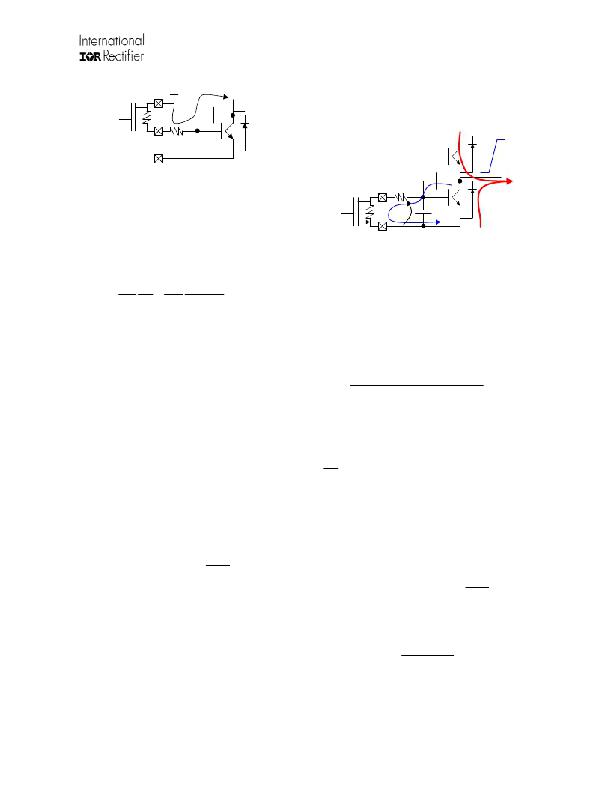
�Figure� 21:� R� Gon� Sizing�
�HS� Turning� ON�
�C� RESoff�
�R� Goff�
�OFF�
�dV/dt�
�where�
�R� TOT� =� R� DRp� +� R� Gon�
�ON�
�R� DRn�
�C� IES�
�R� Gon� =� gate� on-resistor�
�R� DRp� =� driver� equivalent� on-resistance�
�Figure� 22:� R� Goff� Sizing:� Current� Path� When� Low� Side� is�
�R� DRp� is� approximately� given� by�
�Off� and� High� Side� Turns� On�
�R� DRp�
�?� Vcc� t� SW�
�?� I� t�
�=� ?� o� 1� +� on� 1�
�?�
�?� ?�
�+�
�Vcc t� SW� ?� t� on� 1�
�I� o� 2� +� t� SW�
�Vcc�
�I� o� 1� +�
�for� t� SW� >� t� on� 1�
�for� t� SW� ≤� t� on� 1�
�The� transfer� function� between� the� IGBT� collector� and�
�the� IGBT� gate� then� becomes:�
�V� ge� s� ?� (� R� Goff� +� R� DRn� )� ?� C� RESoff�
�=�
�V� de� 1� +� s� ?� (� R� Goff� +� R� DRn� )� ?� (� C� RESoff� +� C� IES� )�
�(I� O1+�
�,I� O2+�
�and�
�t� on1�
�from�
�“Static�
�Electrical�
�Characteristics”).�
�which� yields� to� a� high� pass� filter� with� a� pole� at:�
�Table� 1� reports� the� gate� resistance� size� for� two�
�commonly� used� IGBTs� (calculation� made� using� typical�
�datasheet� values� and� assuming� V� CC� =� 15� V).�
�1� /� τ� =�
�(� R� Goff�
�1�
�+� R� DRn� )� ?� (� C� RESoff� +� C� IES� )�
�Output� Voltage� Slope:� The� turn-on� gate� resistor�
�R� Gon� can� be� sized� to� control� the� output� slope�
�(dV� OUT� /dt).� While� the� output� voltage� has� a� non-�
�linear� behaviour,� the� maximum� output� slope� can� be�
�As� a� result,� when� τ� is� faster� than� the� collector� rise� time�
�(to� be� verified� after� calculation)� the� transfer� function� can�
�be� approximated� by:�
�approximated� by:�
�dV� out�
�dt�
�=�
�I� avg�
�C� RESoff�
�V� ge�
�=� s� ?� (� R� Goff� +� R� DRn� )� ?� C� RESoff�
�V� de�
�so� that�
�Vcc� ?� V� ge�
�C� RESoff� ?�
�V� ge� =� (� R� Goff� +� R� DRn� )� ?� C� RESoff� ?�
�V� th� >� V� ge� =� (� R� Goff� +� R� DRn� )� ?� C� RESoff�
�inserting� the� expression� yielding� I� avg� and� rearranging:�
�*�
�R� TOT� =�
�dV� out�
�dt�
�As� an� example,� table� 2� shows� the� sizing� of� gate�
�resistance� to� get� dV� out� /dt=� 5� V/ns� when� using� two�
�popular� IGBTs� (typical� datasheet� values� are� used� and�
�V� CC� =� 15� V� is� assumed).�
�dV� de�
�dt�
�in� the� time� domain.� Then� the� condition:�
�dV� out�
�dt�
�must� be� verified� to� avoid� spurious� turn� on.�
�Rearranging� the� equation� yields:�
�NOTICE� :� Turn� on� time� must� be� lower� than� T� BL� to� avoid�
�improper� desaturation� detection� and� SSD� triggering.�
�2.6� Sizing� the� Turn-Off� Gate� Resistor�
�The� worst� case� in� sizing� the� turn-off� resistor� R� Goff� is�
�R� Goff� <�
�V� th�
�C� RESoff�
�?�
�dV�
�dt�
�?� R� DRn�
�when� the� collector� of� the� IGBT� in� the� off� state� is� forced�
�to� commutate� by� an� external� event� (e.g.,� the� turn-on� of�
�the� companion� IGBT).� In� this� case� the� dV/dt� of� the�
�output� node� induces� a� parasitic� current� through� C� RESoff�
�www.irf.com�
�18�
�R� DRn� is� approximately� given� by�
�?� 2009� International� Rectifier�
�相关PDF资料 |
PDF描述 |
|---|---|
| IR2118PBF | IC MOSFET DRIVER HIGH-SIDE 8-DIP |
| IR2121PBF | IC MOSFET DRIVER LOW SIDE 8DIP |
| IR2122 | IC MOSFET DRIVER HIGH-SIDE 8-DIP |
| IR2125PBF | IC MOSFET DRIVER LIMITING 8-DIP |
| IR21271PBF | IC DRIVER 600V 200/420MA 8-DIP |
相关代理商/技术参数 |
参数描述 |
|---|---|
| IR21141SSPBF_09 | 制造商:IRF 制造商全称:International Rectifier 功能描述:HALF-BRIDGE GATE DRIVER IC |
| IR21141SSTRPBF | 功能描述:功率驱动器IC 600V Hlf Brdg Drvr IC for Pwr Swtch App RoHS:否 制造商:Micrel 产品:MOSFET Gate Drivers 类型:Low Cost High or Low Side MOSFET Driver 上升时间: 下降时间: 电源电压-最大:30 V 电源电压-最小:2.75 V 电源电流: 最大功率耗散: 最大工作温度:+ 85 C 安装风格:SMD/SMT 封装 / 箱体:SOIC-8 封装:Tube |
| IR2114SS | 功能描述:IC DRIVER HALF-BRIDGE 24-SSOP RoHS:否 类别:集成电路 (IC) >> PMIC - MOSFET,电桥驱动器 - 外部开关 系列:- 标准包装:50 系列:- 配置:高端 输入类型:非反相 延迟时间:200ns 电流 - 峰:250mA 配置数:1 输出数:1 高端电压 - 最大(自引导启动):600V 电源电压:12 V ~ 20 V 工作温度:-40°C ~ 125°C 安装类型:通孔 封装/外壳:8-DIP(0.300",7.62mm) 供应商设备封装:8-DIP 包装:管件 其它名称:*IR2127 |
| IR2114SSPBF | 功能描述:功率驱动器IC 600V HALF BRDG DRVR IC RoHS:否 制造商:Micrel 产品:MOSFET Gate Drivers 类型:Low Cost High or Low Side MOSFET Driver 上升时间: 下降时间: 电源电压-最大:30 V 电源电压-最小:2.75 V 电源电流: 最大功率耗散: 最大工作温度:+ 85 C 安装风格:SMD/SMT 封装 / 箱体:SOIC-8 封装:Tube |
| IR2114SSPBF | 制造商:International Rectifier 功能描述:Driver IC |
发布紧急采购,3分钟左右您将得到回复。