- 您现在的位置:买卖IC网 > Datasheet目录331 > IR21141SSPBF (International Rectifier)IC DRVR HALF BRIDGE 600V 24-SSOP Datasheet资料下载
参数资料
| 型号: | IR21141SSPBF |
| 厂商: | International Rectifier |
| 文件页数: | 20/33页 |
| 文件大小: | 0K |
| 描述: | IC DRVR HALF BRIDGE 600V 24-SSOP |
| 标准包装: | 55 |
| 配置: | 半桥 |
| 输入类型: | 非反相 |
| 延迟时间: | 440ns |
| 电流 - 峰: | 2A |
| 配置数: | 1 |
| 输出数: | 2 |
| 高端电压 - 最大(自引导启动): | 600V |
| 电源电压: | 11.5 V ~ 20 V |
| 工作温度: | -40°C ~ 125°C |
| 安装类型: | 表面贴装 |
| 封装/外壳: | 24-SSOP(0.209",5.30mm 宽) |
| 供应商设备封装: | 24-SSOP |
| 包装: | 管件 |
第1页第2页第3页第4页第5页第6页第7页第8页第9页第10页第11页第12页第13页第14页第15页第16页第17页第18页第19页当前第20页第21页第22页第23页第24页第25页第26页第27页第28页第29页第30页第31页第32页第33页
�� �
�
�IR2114/IR2214SSPbF�
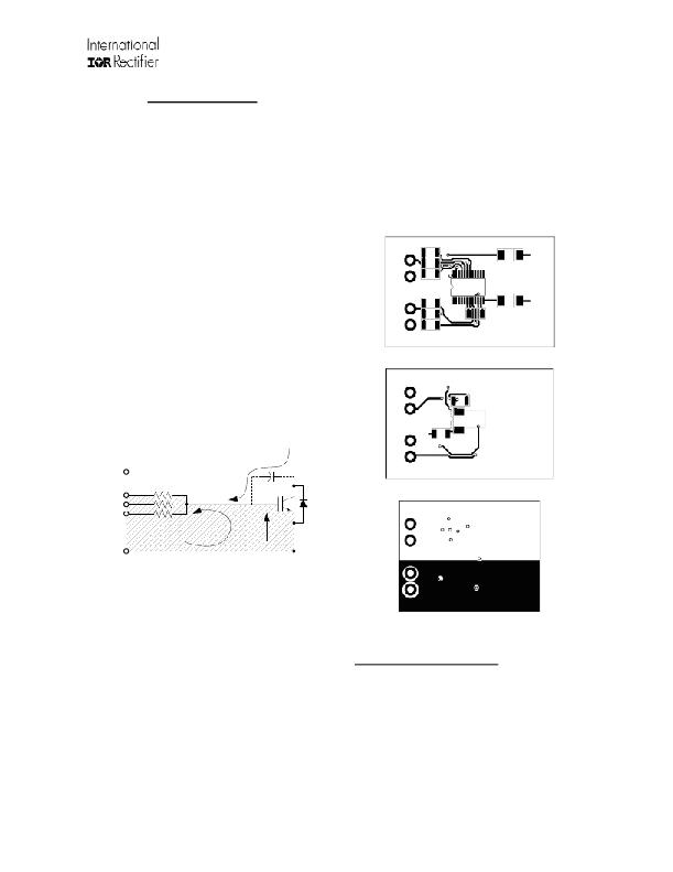
�3 PCB Layout Tips�
�3.5� Routing� and� Placement� Example�
�3.1� Distance� from� High� to� Low� Voltage�
�The� IR2x14x� pinout� maximizes� the� distance� between�
�floating� (from� DC-� to� DC+)� and� low� voltage� pins.� It’s�
�strongly� recommended� to� place� components� tied� to�
�floating� voltage� on� the� high� voltage� side� of� device� (V� B� ,�
�V� S� side)� while� the� other� components� are� placed� on� the�
�opposite� side.�
�3.2� Ground� Plane�
�To� minimize� noise� coupling,� the� ground� plane� must� not�
�be� placed� under� or� near� the� high� voltage� floating� side.�
�Figure� 24� shows� one� of� the� possible� layout� solutions�
�using� a� 3� layer� PCB.� This� example� takes� into� account�
�all� the� previous� considerations.� Placement� and� routing�
�for� supply� capacitors� and� gate� resistances� in� the� high�
�and� low� voltage� side� minimize� the� supply� path� loop� and�
�the� gate� drive� loop.� The� bootstrap� diode� is� placed� under�
�the� device� to� have� the� cathode� as� close� as� possible� to�
�the� bootstrap� capacitor� and� the� anode� far� from� high�
�voltage� and� close� to� V� CC� .�
�3.3� Gate� Drive� Loops�
�V� GH�
�R2�
�R3�
�D2�
�DC+�
�Current� loops� behave� like� antennas� and� are� able� to�
�R4�
�receive� and� transmit� EM� noise.� In� order� to� reduce� the�
�EM� coupling� and� improve� the� power� switch� turn� on/off�
�performances,� gate� drive� loops� must� be� reduced� as�
�V� GL�
�R5�
�IR2214�
�D3�
�Phase�
�much� as� possible.� Figure� 23� shows� the� high� and� low�
�side� gate� loops.�
�Moreover,� current� can� be� injected� inside� the� gate� drive�
�loop� via� the� IGBT� collector-to-gate� parasitic�
�capacitance.� The� parasitic� auto-inductance� of� the� gate�
�loop� contributes� to� developing� a� voltage� across� the�
�gate-emitter,� increasing� the� possibility� of� self� turn-on.�
�For� this� reason,� it� is� strongly� recommended� to� place� the�
�three� gate� resistances� close� together� and� to� minimize�
�the� loop� area� (see� Fig.� 23).�
�I� GC�
�VB/� VCC�
�gate�
�V� EH�
�V� EL�
�R6�
�R7�
�V� CC�
�R1�
�a)�
�C2�
�Top� Layer�
�C1�
�H/LOP�
�H/LON�
�SSDH/L�
�resistance�
�Gate� Drive�
�Loop�
�V� GE�
�C� GC�
�b)� Bottom� Layer�
�VS/COM�
�Figure� 23:� gate� drive� loop�
�3.4� Supply� Capacitors�
�The� IR2x14x� output� stages� are� able� to� quickly� turn� on�
�an� IGBT,� with� up� to� 2� A� of� output� current.� The� supply�
�capacitors� must� be� placed� as� close� as� possible� to� the�
�device� pins� (V� CC� and� V� SS� for� the� ground� tied� supply,� V� B�
�and� V� S� for� the� floating� supply)� in� order� to� minimize�
�parasitic� inductance/resistance.�
�www.irf.com�
�20�
�c)� Ground� Plane�
�Figure� 24:� layout� example�
�Information below refers to Fig. 24:�
�Bootstrap� section:� R1,� C1,� D1�
�High� side� gate:� R2,� R3,� R4�
�High� side� Desat:� D2�
�Low� side� supply:� C2�
�Low� side� gate:� R5,� R6,� R7�
�Low� side� Desat:� D3�
�?� 2009� International� Rectifier�
�相关PDF资料 |
PDF描述 |
|---|---|
| IR2118PBF | IC MOSFET DRIVER HIGH-SIDE 8-DIP |
| IR2121PBF | IC MOSFET DRIVER LOW SIDE 8DIP |
| IR2122 | IC MOSFET DRIVER HIGH-SIDE 8-DIP |
| IR2125PBF | IC MOSFET DRIVER LIMITING 8-DIP |
| IR21271PBF | IC DRIVER 600V 200/420MA 8-DIP |
相关代理商/技术参数 |
参数描述 |
|---|---|
| IR21141SSPBF_09 | 制造商:IRF 制造商全称:International Rectifier 功能描述:HALF-BRIDGE GATE DRIVER IC |
| IR21141SSTRPBF | 功能描述:功率驱动器IC 600V Hlf Brdg Drvr IC for Pwr Swtch App RoHS:否 制造商:Micrel 产品:MOSFET Gate Drivers 类型:Low Cost High or Low Side MOSFET Driver 上升时间: 下降时间: 电源电压-最大:30 V 电源电压-最小:2.75 V 电源电流: 最大功率耗散: 最大工作温度:+ 85 C 安装风格:SMD/SMT 封装 / 箱体:SOIC-8 封装:Tube |
| IR2114SS | 功能描述:IC DRIVER HALF-BRIDGE 24-SSOP RoHS:否 类别:集成电路 (IC) >> PMIC - MOSFET,电桥驱动器 - 外部开关 系列:- 标准包装:50 系列:- 配置:高端 输入类型:非反相 延迟时间:200ns 电流 - 峰:250mA 配置数:1 输出数:1 高端电压 - 最大(自引导启动):600V 电源电压:12 V ~ 20 V 工作温度:-40°C ~ 125°C 安装类型:通孔 封装/外壳:8-DIP(0.300",7.62mm) 供应商设备封装:8-DIP 包装:管件 其它名称:*IR2127 |
| IR2114SSPBF | 功能描述:功率驱动器IC 600V HALF BRDG DRVR IC RoHS:否 制造商:Micrel 产品:MOSFET Gate Drivers 类型:Low Cost High or Low Side MOSFET Driver 上升时间: 下降时间: 电源电压-最大:30 V 电源电压-最小:2.75 V 电源电流: 最大功率耗散: 最大工作温度:+ 85 C 安装风格:SMD/SMT 封装 / 箱体:SOIC-8 封装:Tube |
| IR2114SSPBF | 制造商:International Rectifier 功能描述:Driver IC |
发布紧急采购,3分钟左右您将得到回复。