- 您现在的位置:买卖IC网 > PDF目录21788 > IRF7807VD2PBF (International Rectifier)MOSFET N-CH 30V 8.3A 8-SOIC PDF资料下载
参数资料
| 型号: | IRF7807VD2PBF |
| 厂商: | International Rectifier |
| 文件页数: | 3/9页 |
| 文件大小: | 0K |
| 描述: | MOSFET N-CH 30V 8.3A 8-SOIC |
| 标准包装: | 95 |
| 系列: | FETKY™ |
| FET 型: | MOSFET N 通道,金属氧化物 |
| FET 特点: | 二极管(隔离式) |
| 漏极至源极电压(Vdss): | 30V |
| 电流 - 连续漏极(Id) @ 25° C: | 8.3A |
| 开态Rds(最大)@ Id, Vgs @ 25° C: | 25 毫欧 @ 7A,4.5V |
| Id 时的 Vgs(th)(最大): | 1V @ 250µA |
| 闸电荷(Qg) @ Vgs: | 14nC @ 4.5V |
| 功率 - 最大: | 2.5W |
| 安装类型: | 表面贴装 |
| 封装/外壳: | 8-SOIC(0.154",3.90mm 宽) |
| 供应商设备封装: | 8-SO |
| 包装: | 管件 |
�� �
�
�IRF7807VD2PbF�
�Power� MOSFET� Selection� for� DC/DC�
�Converters�
�Control� FET�
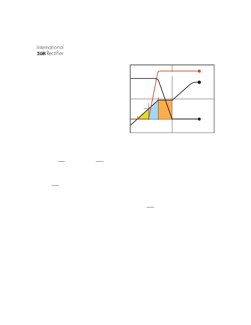
�Drain� Current�
�4�
�Special� attention� has� been� given� to� the� power� losses�
�in� the� switching� elements� of� the� circuit� -� Q1� and� Q2.�
�1�
�Gate� Voltage�
�Power� losses� in� the� high� side� switch� Q1,� also� called�
�the� Control� FET,� are� impacted� by� the� R� ds(on)� of� the�
�MOSFET,� but� these� conduction� losses� are� only� about�
�one� half� of� the� total� losses.�
�t1�
�V� GTH�
�t2�
�t3�
�Power� losses� in� the� control� switch� Q1� are� given�
�by;�
�t0�
�2�
�Drain� Voltage�
�P� loss� =� P� conduction� +� P� switching� +� P� drive� +� P� output�
�This� can� be� expanded� and� approximated� by;�
�� V� in� � f� ?�
�P� loss� =� (� I� rms 2� � R� ds(on)� )�
�?� Q� gd� ?� ?�
�+� ?� I� � � V� in� � f� ?� +� ?� I� �
�?� i� g� ?� ?�
�Q� gs� 2�
�i� g�
�?�
�?�
�Figure� 1:� Typical� MOSFET� switching� waveform�
�Synchronous� FET�
�The� power� loss� equation� for� Q2� is� approximated�
�by;�
�� V� in� � f� ?�
�?� Q� oss�
�?� 2�
�?�
�P� loss� =� P� conduction� +� P� drive� +� P� output�
�(� )�
�P� loss� =� I� rms� � R� ds(on)�
�+� ?� oss� � V� in� � f� +� (� Q� rr� � V� in� � f� )�
�+� (� Q� g� � V� g� � f� )�
�+�
�This� simplified� loss� equation� includes� the� terms� Q� gs2�
�and� Q� oss� which� are� new� to� Power� MOSFET� data� sheets.�
�Q� gs2� is� a� sub� element� of� traditional� gate-source�
�charge� that� is� included� in� all� MOSFET� data� sheets.�
�The� importance� of� splitting� this� gate-source� charge�
�into� two� sub� elements,� Q� gs1� and� Q� gs2� ,� can� be� seen� from�
�Fig� 1.�
�Q� gs2� indicates� the� charge� that� must� be� supplied� by�
�the� gate� driver� between� the� time� that� the� threshold�
�voltage� has� been� reached� (t1)� and� the� time� the� drain�
�current� rises� to� I� dmax� (t2)� at� which� time� the� drain� volt-�
�age� begins� to� change.� Minimizing� Q� gs2� is� a� critical� fac-�
�tor� in� reducing� switching� losses� in� Q1.�
�Q� oss� is� the� charge� that� must� be� supplied� to� the� out-�
�put� capacitance� of� the� MOSFET� during� every� switch-�
�ing� cycle.� Figure� 2� shows� how� Q� oss� is� formed� by� the�
�parallel� combination� of� the� voltage� dependant� (non-�
�linear)� capacitance’s� C� ds� and� C� dg� when� multiplied� by�
�the� power� supply� input� buss� voltage.�
�www.irf.com�
�2�
�+� (� Q� g� � V� g� � f� )�
�?� Q� ?�
�?� 2� ?�
�*dissipated� primarily� in� Q1.�
�*�
�3�
�相关PDF资料 |
PDF描述 |
|---|---|
| 445W25D24M00000 | CRYSTAL 24.00000 MHZ 18PF SMD |
| A13AH | SW TOGGLE SPDT RT ANG BRKT PCB |
| IRLR3717TRPBF | MOSFET N-CH 20V 120A DPAK |
| M2T12SA5G13 | SW TOGGLE SPDT .500" GOLD PCB |
| 445W25A24M00000 | CRYSTAL 24.00000 MHZ 10PF SMD |
相关代理商/技术参数 |
参数描述 |
|---|---|
| IRF7807VD2TR | 功能描述:MOSFET N-CH 30V 8.3A 8-SOIC RoHS:否 类别:分离式半导体产品 >> FET - 单 系列:FETKY™ 标准包装:1,000 系列:MESH OVERLAY™ FET 型:MOSFET N 通道,金属氧化物 FET 特点:逻辑电平门 漏极至源极电压(Vdss):200V 电流 - 连续漏极(Id) @ 25° C:18A 开态Rds(最大)@ Id, Vgs @ 25° C:180 毫欧 @ 9A,10V Id 时的 Vgs(th)(最大):4V @ 250µA 闸电荷(Qg) @ Vgs:72nC @ 10V 输入电容 (Ciss) @ Vds:1560pF @ 25V 功率 - 最大:40W 安装类型:通孔 封装/外壳:TO-220-3 整包 供应商设备封装:TO-220FP 包装:管件 |
| IRF7807VD2TRPBF | 功能描述:MOSFET MOSFT w/Schttky 30V 8.3A 25mOhm 9.5nC RoHS:否 制造商:STMicroelectronics 晶体管极性:N-Channel 汲极/源极击穿电压:650 V 闸/源击穿电压:25 V 漏极连续电流:130 A 电阻汲极/源极 RDS(导通):0.014 Ohms 配置:Single 最大工作温度: 安装风格:Through Hole 封装 / 箱体:Max247 封装:Tube |
| IRF7807VPBF | 功能描述:MOSFET 30V 1 N-CH HEXFET 25mOhms 9.5nC RoHS:否 制造商:STMicroelectronics 晶体管极性:N-Channel 汲极/源极击穿电压:650 V 闸/源击穿电压:25 V 漏极连续电流:130 A 电阻汲极/源极 RDS(导通):0.014 Ohms 配置:Single 最大工作温度: 安装风格:Through Hole 封装 / 箱体:Max247 封装:Tube |
| IRF7807VTR | 功能描述:MOSFET N-CH 30V 8.3A 8-SOIC RoHS:否 类别:分离式半导体产品 >> FET - 单 系列:HEXFET® 标准包装:1,000 系列:MESH OVERLAY™ FET 型:MOSFET N 通道,金属氧化物 FET 特点:逻辑电平门 漏极至源极电压(Vdss):200V 电流 - 连续漏极(Id) @ 25° C:18A 开态Rds(最大)@ Id, Vgs @ 25° C:180 毫欧 @ 9A,10V Id 时的 Vgs(th)(最大):4V @ 250µA 闸电荷(Qg) @ Vgs:72nC @ 10V 输入电容 (Ciss) @ Vds:1560pF @ 25V 功率 - 最大:40W 安装类型:通孔 封装/外壳:TO-220-3 整包 供应商设备封装:TO-220FP 包装:管件 |
| IRF7807VTRPBF | 功能描述:MOSFET MOSFT 30V 8.3A 25mOhm 9.5nC RoHS:否 制造商:STMicroelectronics 晶体管极性:N-Channel 汲极/源极击穿电压:650 V 闸/源击穿电压:25 V 漏极连续电流:130 A 电阻汲极/源极 RDS(导通):0.014 Ohms 配置:Single 最大工作温度: 安装风格:Through Hole 封装 / 箱体:Max247 封装:Tube |
发布紧急采购,3分钟左右您将得到回复。