- 您现在的位置:买卖IC网 > PDF目录21788 > IRF7807VD2PBF (International Rectifier)MOSFET N-CH 30V 8.3A 8-SOIC PDF资料下载
参数资料
| 型号: | IRF7807VD2PBF |
| 厂商: | International Rectifier |
| 文件页数: | 4/9页 |
| 文件大小: | 0K |
| 描述: | MOSFET N-CH 30V 8.3A 8-SOIC |
| 标准包装: | 95 |
| 系列: | FETKY™ |
| FET 型: | MOSFET N 通道,金属氧化物 |
| FET 特点: | 二极管(隔离式) |
| 漏极至源极电压(Vdss): | 30V |
| 电流 - 连续漏极(Id) @ 25° C: | 8.3A |
| 开态Rds(最大)@ Id, Vgs @ 25° C: | 25 毫欧 @ 7A,4.5V |
| Id 时的 Vgs(th)(最大): | 1V @ 250µA |
| 闸电荷(Qg) @ Vgs: | 14nC @ 4.5V |
| 功率 - 最大: | 2.5W |
| 安装类型: | 表面贴装 |
| 封装/外壳: | 8-SOIC(0.154",3.90mm 宽) |
| 供应商设备封装: | 8-SO |
| 包装: | 管件 |
�� �
�
�IRF7807VD2PbF�
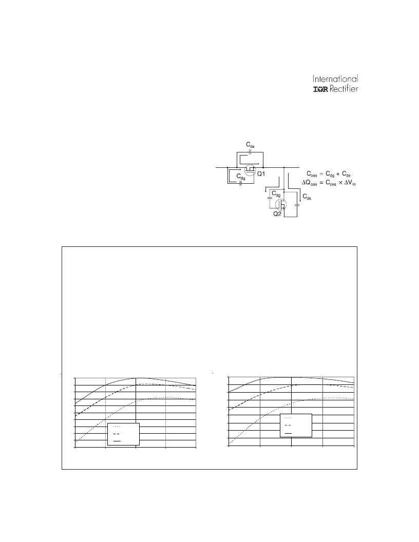
�For� the� synchronous� MOSFET� Q2,� R� ds(on)� is� an� im-�
�portant� characteristic;� however,� once� again� the� im-�
�portance� of� gate� charge� must� not� be� overlooked� since�
�it� impacts� three� critical� areas.� Under� light� load� the�
�MOSFET� must� still� be� turned� on� and� off� by� the� con-�
�trol� IC� so� the� gate� drive� losses� become� much� more�
�significant.� Secondly,� the� output� charge� Q� oss� and� re-�
�verse� recovery� charge� Q� rr� both� generate� losses� that�
�are� transfered� to� Q1� and� increase� the� dissipation� in�
�that� device.� Thirdly,� gate� charge� will� impact� the�
�MOSFETs’� susceptibility� to� Cdv/dt� turn� on.�
�The� drain� of� Q2� is� connected� to� the� switching� node�
�of� the� converter� and� therefore� sees� transitions� be-�
�tween� ground� and� V� in� .� As� Q1� turns� on� and� off� there� is�
�a� rate� of� change� of� drain� voltage� dV/dt� which� is� ca-�
�pacitively� coupled� to� the� gate� of� Q2� and� can� induce�
�a� voltage� spike� on� the� gate� that� is� sufficient� to� turn�
�Typical� Mobile� PC� Application�
�The� performance� of� these� new� devices� has� been� tested�
�in� circuit� and� correlates� well� with� performance� predic-�
�tions� generated� by� the� system� models.� An� advantage� of�
�this� new� technology� platform� is� that� the� MOSFETs� it�
�produces� are� suitable� for� both� control� FET� and� synchro-�
�nous� FET� applications.� This� has� been� demonstrated� with�
�the� 3.3V� and� 5V� converters.� (Fig� 3� and� Fig� 4).� In� these�
�applications� the� same� MOSFET� IRF7807V� was� used� for�
�both� the� control� FET� (Q1)� and� the� synchronous� FET�
�(Q2).� This� provides� a� highly� effective� cost/performance�
�solution.�
�3.3V� Supply� :� Q1=Q2=� IRF7807V�
�93�
�92�
�91�
�90�
�89�
�the� MOSFET� on,� resulting� in� shoot-through� current� .�
�The� ratio� of� Q� gd� /Q� gs1� must� be� minimized� to� reduce� the�
�potential� for� Cdv/dt� turn� on.�
�Spice� model� for� IRF7807V� can� be� downloaded� in�
�machine� readable� format� at� www.irf.com.�
�Figure� 2:� Q� oss� Characteristic�
�5.0V� Supply� :� Q1=Q2=� IRF7807V�
�95�
�94�
�93�
�92�
�91�
�88�
�87�
�86�
�85�
�84�
�83�
�Vin=24V�
�Vin=14V�
�Vin=10V�
�90�
�89�
�88�
�87�
�86�
�Vin=24V�
�Vin=14V�
�Vin=10V�
�1�
�2�
�3�
�Load� current� (A)�
�4�
�5�
�1�
�2�
�3�
�Load� current� (A)�
�4�
�5�
�4�
�Figure� 3�
�Figure� 4�
�www.irf.com�
�相关PDF资料 |
PDF描述 |
|---|---|
| 445W25D24M00000 | CRYSTAL 24.00000 MHZ 18PF SMD |
| A13AH | SW TOGGLE SPDT RT ANG BRKT PCB |
| IRLR3717TRPBF | MOSFET N-CH 20V 120A DPAK |
| M2T12SA5G13 | SW TOGGLE SPDT .500" GOLD PCB |
| 445W25A24M00000 | CRYSTAL 24.00000 MHZ 10PF SMD |
相关代理商/技术参数 |
参数描述 |
|---|---|
| IRF7807VD2TR | 功能描述:MOSFET N-CH 30V 8.3A 8-SOIC RoHS:否 类别:分离式半导体产品 >> FET - 单 系列:FETKY™ 标准包装:1,000 系列:MESH OVERLAY™ FET 型:MOSFET N 通道,金属氧化物 FET 特点:逻辑电平门 漏极至源极电压(Vdss):200V 电流 - 连续漏极(Id) @ 25° C:18A 开态Rds(最大)@ Id, Vgs @ 25° C:180 毫欧 @ 9A,10V Id 时的 Vgs(th)(最大):4V @ 250µA 闸电荷(Qg) @ Vgs:72nC @ 10V 输入电容 (Ciss) @ Vds:1560pF @ 25V 功率 - 最大:40W 安装类型:通孔 封装/外壳:TO-220-3 整包 供应商设备封装:TO-220FP 包装:管件 |
| IRF7807VD2TRPBF | 功能描述:MOSFET MOSFT w/Schttky 30V 8.3A 25mOhm 9.5nC RoHS:否 制造商:STMicroelectronics 晶体管极性:N-Channel 汲极/源极击穿电压:650 V 闸/源击穿电压:25 V 漏极连续电流:130 A 电阻汲极/源极 RDS(导通):0.014 Ohms 配置:Single 最大工作温度: 安装风格:Through Hole 封装 / 箱体:Max247 封装:Tube |
| IRF7807VPBF | 功能描述:MOSFET 30V 1 N-CH HEXFET 25mOhms 9.5nC RoHS:否 制造商:STMicroelectronics 晶体管极性:N-Channel 汲极/源极击穿电压:650 V 闸/源击穿电压:25 V 漏极连续电流:130 A 电阻汲极/源极 RDS(导通):0.014 Ohms 配置:Single 最大工作温度: 安装风格:Through Hole 封装 / 箱体:Max247 封装:Tube |
| IRF7807VTR | 功能描述:MOSFET N-CH 30V 8.3A 8-SOIC RoHS:否 类别:分离式半导体产品 >> FET - 单 系列:HEXFET® 标准包装:1,000 系列:MESH OVERLAY™ FET 型:MOSFET N 通道,金属氧化物 FET 特点:逻辑电平门 漏极至源极电压(Vdss):200V 电流 - 连续漏极(Id) @ 25° C:18A 开态Rds(最大)@ Id, Vgs @ 25° C:180 毫欧 @ 9A,10V Id 时的 Vgs(th)(最大):4V @ 250µA 闸电荷(Qg) @ Vgs:72nC @ 10V 输入电容 (Ciss) @ Vds:1560pF @ 25V 功率 - 最大:40W 安装类型:通孔 封装/外壳:TO-220-3 整包 供应商设备封装:TO-220FP 包装:管件 |
| IRF7807VTRPBF | 功能描述:MOSFET MOSFT 30V 8.3A 25mOhm 9.5nC RoHS:否 制造商:STMicroelectronics 晶体管极性:N-Channel 汲极/源极击穿电压:650 V 闸/源击穿电压:25 V 漏极连续电流:130 A 电阻汲极/源极 RDS(导通):0.014 Ohms 配置:Single 最大工作温度: 安装风格:Through Hole 封装 / 箱体:Max247 封装:Tube |
发布紧急采购,3分钟左右您将得到回复。