- 您现在的位置:买卖IC网 > PDF目录384498 > IRFSL4310ZPBF (International Rectifier) HEXFET Power MOSFET PDF资料下载
参数资料
| 型号: | IRFSL4310ZPBF |
| 厂商: | International Rectifier |
| 英文描述: | HEXFET Power MOSFET |
| 中文描述: | HEXFET功率MOSFET |
| 文件页数: | 2/11页 |
| 文件大小: | 437K |
| 代理商: | IRFSL4310ZPBF |
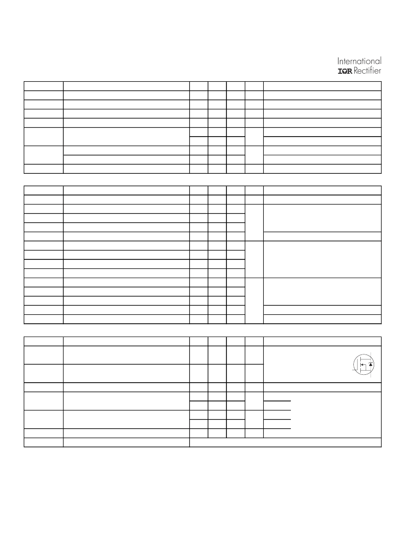
2
www.irf.com
Calculated continuous current based on maximum allowable junction
temperature. Package limitation current is 75A
Repetitive rating; pulse width limited by max. junction
temperature.
Limited by T
Jmax
, starting T
J
= 25°C, L = 0.047mH
R
G
= 25
Ω
, I
AS
= 75A, V
GS
=10V. Part not recommended for use
above this value.
I
SD
≤
75A, di/dt
≤
600A/
μ
s, V
DD
≤
V
(BR)DSS
, T
J
≤
175°C.
Pulse width
≤
400
μ
s; duty cycle
≤
2%.
S
D
G
C
oss
eff. (TR) is a fixed capacitance that gives the same charging time
as C
oss
while V
DS
is rising from 0 to 80% V
DSS
.
C
oss
eff. (ER) is a fixed capacitance that gives the same energy as
C
oss
while V
DS
is rising from 0 to 80% V
DSS
.
When mounted on 1" square PCB (FR-4 or G-10 Material). For recom
mended footprint and soldering techniques refer to application note #AN-994.
θ
Static @ T
J
= 25°C (unless otherwise specified)
Symbol
V
(BR)DSS
Drain-to-Source Breakdown Voltage
Δ
V
(BR)DSS
/
Δ
T
J
Breakdown Voltage Temp. Coefficient
R
DS(on)
Static Drain-to-Source On-Resistance
V
GS(th)
Gate Threshold Voltage
I
DSS
Drain-to-Source Leakage Current
Parameter
Min. Typ. Max. Units
100
–––
–––
0.11
–––
4.8
2.0
–––
–––
–––
–––
–––
–––
–––
–––
–––
–––
0.7
–––
–––
6.0
4.0
20
250
100
-100
–––
V
V/°C
m
Ω
V
μ
A
I
GSS
Gate-to-Source Forward Leakage
Gate-to-Source Reverse Leakage
Internal Gate Resistance
nA
R
G
Dynamic @ T
J
= 25°C (unless otherwise specified)
Symbol
Parameter
gfs
Forward Transconductance
Q
g
Total Gate Charge
Q
gs
Gate-to-Source Charge
Q
gd
Gate-to-Drain ("Miller") Charge
Q
sync
Total Gate Charge Sync. (Q
g
- Q
gd
)
t
d(on)
Turn-On Delay Time
t
r
Rise Time
t
d(off)
Turn-Off Delay Time
t
f
Fall Time
C
iss
Input Capacitance
C
oss
Output Capacitance
C
rss
Reverse Transfer Capacitance
C
oss
eff. (ER) Effective Output Capacitance (Energy Related) –––
C
oss
eff. (TR)
Effective Output Capacitance (Time Related)
Ω
Min. Typ. Max. Units
150
–––
–––
120
–––
29
–––
35
–––
85
–––
20
–––
60
–––
55
–––
57
–––
6860
–––
490
–––
220
570
–––
920
–––
170
–––
S
nC
–––
–––
–––
–––
–––
–––
–––
–––
–––
–––
ns
pF
Diode Characteristics
Symbol
I
S
Parameter
Continuous Source Current
Min. Typ. Max. Units
–––
–––
127
A
(Body Diode)
Pulsed Source Current
I
SM
–––
–––
560
A
(Body Diode)
Diode Forward Voltage
Reverse Recovery Time
V
SD
t
rr
–––
–––
–––
–––
–––
–––
Intrinsic turn-on time is negligible (turn-on is dominated by LS+LD)
–––
40
49
58
89
2.5
1.3
V
ns
T
J
= 25°C
T
J
= 125°C
T
J
= 25°C
T
J
= 125°C
T
J
= 25°C
V
R
= 85V,
I
F
= 75A
di/dt = 100A/
μ
s
Q
rr
Reverse Recovery Charge
nC
I
RRM
t
on
Reverse Recovery Current
Forward Turn-On Time
–––
A
I
D
= 75A
R
G
= 2.7
Ω
V
GS
= 10V
V
GS
= 0V
V
DS
= 50V
= 1.0MHz, See Fig. 5
V
GS
= 0V, V
DS
= 0V to 80V , See Fig. 11
V
GS
= 0V, V
DS
= 0V to 80V
V
GS
= 10V
I
D
= 75A, V
DS
=0V, V
GS
= 10V
V
DD
= 65V
T
J
= 25°C, I
S
= 75A, V
GS
= 0V
integral reverse
p-n junction diode.
Conditions
V
GS
= 0V, I
D
= 250
μ
A
Reference to 25°C, I
D
= 5mA
V
GS
= 10V, I
D
= 75A
V
DS
= V
GS
, I
D
= 150
μ
A
V
DS
= 100V, V
GS
= 0V
V
DS
= 80V, V
GS
= 0V, T
J
= 125°C
V
GS
= 20V
V
GS
= -20V
MOSFET symbol
showing the
V
DS
=50V
Conditions
Conditions
V
DS
= 50V, I
D
= 75A
I
D
= 75A
相关PDF资料 |
PDF描述 |
|---|---|
| IRFS4410ZPBF | HEXFET Power MOSFET |
| IRFSL4410ZPBF | HEXFET Power MOSFET |
| IRFS9N60APBF | SMPS MOSFET |
| IRFS9N60A | SMPS MOSFET |
| IRFSL9N60A | SMPS MOSFET |
相关代理商/技术参数 |
参数描述 |
|---|---|
| IRFSL4321PBF | 功能描述:MOSFET MOSFT 150V 83A 15mOhm 71nC RoHS:否 制造商:STMicroelectronics 晶体管极性:N-Channel 汲极/源极击穿电压:650 V 闸/源击穿电压:25 V 漏极连续电流:130 A 电阻汲极/源极 RDS(导通):0.014 Ohms 配置:Single 最大工作温度: 安装风格:Through Hole 封装 / 箱体:Max247 封装:Tube |
| IRFSL4410 | 功能描述:MOSFET N-CH 100V 96A TO-262 RoHS:否 类别:分离式半导体产品 >> FET - 单 系列:HEXFET® 标准包装:1,000 系列:MESH OVERLAY™ FET 型:MOSFET N 通道,金属氧化物 FET 特点:逻辑电平门 漏极至源极电压(Vdss):200V 电流 - 连续漏极(Id) @ 25° C:18A 开态Rds(最大)@ Id, Vgs @ 25° C:180 毫欧 @ 9A,10V Id 时的 Vgs(th)(最大):4V @ 250µA 闸电荷(Qg) @ Vgs:72nC @ 10V 输入电容 (Ciss) @ Vds:1560pF @ 25V 功率 - 最大:40W 安装类型:通孔 封装/外壳:TO-220-3 整包 供应商设备封装:TO-220FP 包装:管件 |
| IRFSL4410PBF | 功能描述:MOSFET MOSFT 100V 96A 10mOhm 120nC RoHS:否 制造商:STMicroelectronics 晶体管极性:N-Channel 汲极/源极击穿电压:650 V 闸/源击穿电压:25 V 漏极连续电流:130 A 电阻汲极/源极 RDS(导通):0.014 Ohms 配置:Single 最大工作温度: 安装风格:Through Hole 封装 / 箱体:Max247 封装:Tube |
| IRFSL4410ZPBF | 功能描述:MOSFET MOSFT 100V 97A 9mOhm 83nC RoHS:否 制造商:STMicroelectronics 晶体管极性:N-Channel 汲极/源极击穿电压:650 V 闸/源击穿电压:25 V 漏极连续电流:130 A 电阻汲极/源极 RDS(导通):0.014 Ohms 配置:Single 最大工作温度: 安装风格:Through Hole 封装 / 箱体:Max247 封装:Tube |
| IRFSL4510PBF | 功能描述:MOSFET N CH 100V TO262 RoHS:是 类别:分离式半导体产品 >> FET - 单 系列:HEXFET® 标准包装:1,000 系列:MESH OVERLAY™ FET 型:MOSFET N 通道,金属氧化物 FET 特点:逻辑电平门 漏极至源极电压(Vdss):200V 电流 - 连续漏极(Id) @ 25° C:18A 开态Rds(最大)@ Id, Vgs @ 25° C:180 毫欧 @ 9A,10V Id 时的 Vgs(th)(最大):4V @ 250µA 闸电荷(Qg) @ Vgs:72nC @ 10V 输入电容 (Ciss) @ Vds:1560pF @ 25V 功率 - 最大:40W 安装类型:通孔 封装/外壳:TO-220-3 整包 供应商设备封装:TO-220FP 包装:管件 |
发布紧急采购,3分钟左右您将得到回复。