参数资料
| 型号: | ISL6227IRZ |
| 厂商: | Intersil |
| 文件页数: | 15/27页 |
| 文件大小: | 0K |
| 描述: | IC CONTROLLER DDR, DDR2 28QFN |
| 标准包装: | 60 |
| 应用: | 控制器,DDR,DDR2 |
| 输入电压: | 5 V ~ 28 V |
| 输出数: | 2 |
| 输出电压: | 0.9 V ~ 5.5 V |
| 工作温度: | -40°C ~ 100°C |
| 安装类型: | 表面贴装 |
| 封装/外壳: | 28-VFQFN 裸露焊盘 |
| 供应商设备封装: | 28-QFN 裸露焊盘(5x5) |
| 包装: | 管件 |
第1页第2页第3页第4页第5页第6页第7页第8页第9页第10页第11页第12页第13页第14页当前第15页第16页第17页第18页第19页第20页第21页第22页第23页第24页第25页第26页第27页
�� �
�
�ISL6227�
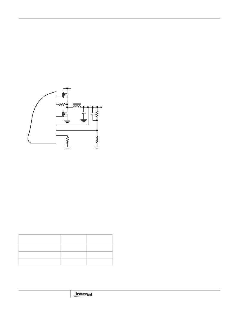
�Output� Voltage� Program�
�The� output� voltage� of� either� channel� is� set� by� a� resistive� divider�
�from� the� output� to� ground.� The� center� point� of� the� divider� is�
�connected� to� the� VSEN� pin� as� shown� in� Figure� 34.� The�
�output� voltage� value� is� determined� by� Equation� 3:�
�The� two� channels� can� be� programmed� to� operate� in� different�
�modes� depending� on� the� VOUTx� connection� and� the� load�
�current.� Once� both� channels� operate� in� the� PWM� mode,�
�however,� they� will� be� synchronized� to� the� 300kHz� switching�
�clock.� The� 180°� phase� shift� reduces� the� noise� couplings�
�V� O� =� ----------------------------------------------�
�0.9V� ?� (� R1� +� R2� )�
�R2�
�(EQ.� 3)�
�between� the� two� channels� and� reduces� the� input� current� ripple.�
�The� critical� discontinuous� conduction� current� value� for� the�
�PWM� to� HYS� mode� switch-over� can� be� calculated� by�
�where� 0.9V� is� the� value� of� the� internal� reference.� The� VSEN�
�Equation� 4:�
�2� ?� F� SW� ?� L� O� ?� V� IN�
�pin� voltage� is� also� used� by� the� controller� for� the� power� good�
�function� and� to� detect� undervoltage� and� overvoltage�
�conditions.�
�(� V� IN� –� V� O� )� ?� V� O�
�I� HYS� =� ----------------------------------------------------�
�(EQ.� 4)�
�Q1�
�V� IN�
�The� HYS� mode� to� PWM� switch-over� current� I� HYS1� is�
�determined� by� the� activation� time� of� the� HYS� mode�
�controller.� It� is� affected� by� the� ESR,� the� inductor� value,� the�
�UGATE�
�ISEN�
�R� CS�
�L1�
�V� O�
�input� and� output� voltage.�
�The� HYS� mode� control� can� improve� converter� efficiency� with�
�LGATE�
�Q2�
�C1�
�C� Z�
�R1�
�reduced� switching� frequency.� The� efficiency� is� further�
�improved� by� the� diode� emulation� scheme� in� discontinuous�
�conduction� mode.� The� diode� emulation� scheme� does� not�
�VOUT�
�VSEN�
�allow� the� inductor� sink� current� from� the� output� capacitor,�
�thereby� reducing� the� circulating� energy.� It� is� achieved� by�
�sensing� the� free-wheeling� current� going� through� the�
�ISL6227�
�OCSET�
�R� OC�
�R2�
�synchronous� MOSFET� through� Phase� node� voltage� polarity�
�change� after� the� upper� MOSFET� is� turned� off.� Before� the�
�current� reverses� direction,� the� lower� MOSFET� gate� pulses�
�are� terminated.�
�FIGURE� 34.� OUTPUT� VOLTAGE� PROGRAM�
�Operation� Mode� Control�
�VOUTx� pin� programs� the� two� channels� of� ISL6227� in� two�
�different� operational� modes:�
�1.� If� VOUTx� is� connected� to� ground,� the� channel� will� be� put�
�into� a� fixed� switching� frequency� of� 300kHz� CCM,� also�
�known� as� forced� PWM� mode� regardless� of� load�
�conditions.�
�2.� If� the� VOUTx� is� connected� to� the� output� voltage,� the�
�channel� will� operate� in� either� fixed� 300kHz� PWM� mode� or�
�HYS� mode,� depending� on� the� load� conditions.� It� operates�
�in� the� PWM� mode� when� the� load� current� exceeds� the�
�critical� discontinuous� conduction� value,� otherwise� it� will�
�operate� in� a� HYS� mode,� as� shown� in� the� following� table.�
�The� PWM-HYS� and� HYS-PWM� switch-over� is� provided�
�automatically� by� the� mode� control� circuit,� which� constantly�
�monitors� the� inductor� current� through� phase� voltage� polarity,�
�and� alters� the� way� the� gate� driver� pulse� signal� is� generated.�
�Mode� Transition�
�For� a� buck� regulator,� if� the� load� current� is� higher� than� critical�
�value� I� HYS1� ,� the� voltage� drop� on� the� synchronous� MOSFET�
�in� the� free-wheeling� period� is� always� negative,� and� vice�
�versa.� The� mode� control� circuit� monitors� the� phase� node�
�voltage� in� the� off-period.� The� polarity� of� this� voltage� is� used�
�as� the� criteria� for� whether� the� load� current� is� greater� than� the�
�critical� value,� and� thus� determines� whether� the� converter� will�
�operate� in� PWM� or� HYS� mode.�
�To� prevent� chatter� between� operating� modes,� the� circuit�
�looks� for� eight� sequentially� matching� polarity� signals� before� it�
�VOUT� PIN�
�GND�
�Connects� to� output� voltage�
�Connects� to� output� voltage�
�INDUCTOR�
�CURRENT�
�Any� value�
�≤� I� HYS�
�>I� HYS1�
�OPERATION�
�MODE�
�Forced� PWM�
�HYS�
�PWM�
�decides� to� perform� a� mode� change.� The� algorithm� is� true� for�
�both� CCM-HYS� and� HYS-CCM� transitions.�
�In� the� HYS� mode,� the� PWM� comparator� and� the� error�
�amplifier,� that� provided� control� in� the� CCM� mode,� are� put� in� a�
�clamped� stage� and� the� hysteretic� comparator� is� activated.� A�
�change� is� also� made� to� the� gate� logic.� The� synchronous�
�MOSFET� is� controlled� in� diode� emulation� fashion,� hence� the�
�current� in� the� synchronous� MOSFET� will� be� kept� in� one�
�direction� only.� Figures� 35� and� 36� illustrate� the� mode� change�
�by� counting� eight� switching� cycles.�
�15�
�FN9094.7�
�May� 4,� 2009�
�相关PDF资料 |
PDF描述 |
|---|---|
| 80MXC5600MEFCSN35X40 | CAP ALUM 5600UF 80V 20% SNAP-IN |
| EL5126CLZ-T13 | IC VOLTAGE GEN 8CH TFT-LCD 32QFN |
| 250MXC1000MEFCSN35X35 | CAP ALUM 1000UF 250V 20% SNAP-IN |
| EL5126CLZ-T7 | IC VOLTAGE GEN 8CH TFT-LCD 32QFN |
| 400SXC330MEFCSN30X45 | CAP ALUM 330UF 400V 20% SNAP-IN |
相关代理商/技术参数 |
参数描述 |
|---|---|
| ISL6227IRZ-T | 功能描述:IC CONTROLLER DDR, DDR2 28QFN RoHS:是 类别:集成电路 (IC) >> PMIC - 稳压器 - 专用型 系列:- 标准包装:43 系列:- 应用:控制器,Intel VR11 输入电压:5 V ~ 12 V 输出数:1 输出电压:0.5 V ~ 1.6 V 工作温度:-40°C ~ 85°C 安装类型:表面贴装 封装/外壳:48-VFQFN 裸露焊盘 供应商设备封装:48-QFN(7x7) 包装:管件 |
| ISL6228 | 制造商:INTERSIL 制造商全称:Intersil Corporation 功能描述:High-Performance Dual-Output Buck Controller for Notebook Applications |
| ISL6228EVAL3Z | 功能描述:EVALUATION BOARD FOR ISL6228 RoHS:是 类别:编程器,开发系统 >> 评估板 - DC/DC 与 AC/DC(离线)SMPS 系列:Robust Ripple Regulator™ (R³) 产品培训模块:Obsolescence Mitigation Program 标准包装:1 系列:True Shutdown™ 主要目的:DC/DC,步升 输出及类型:1,非隔离 功率 - 输出:- 输出电压:- 电流 - 输出:1A 输入电压:2.5 V ~ 5.5 V 稳压器拓扑结构:升压 频率 - 开关:3MHz 板类型:完全填充 已供物品:板 已用 IC / 零件:MAX8969 |
| ISL6228HIEVAL3Z | 功能描述:EVALUATION BOARD FOR ISL6228HI RoHS:是 类别:编程器,开发系统 >> 评估板 - DC/DC 与 AC/DC(离线)SMPS 系列:Robust Ripple Regulator™ (R³) 产品培训模块:Obsolescence Mitigation Program 标准包装:1 系列:True Shutdown™ 主要目的:DC/DC,步升 输出及类型:1,非隔离 功率 - 输出:- 输出电压:- 电流 - 输出:1A 输入电压:2.5 V ~ 5.5 V 稳压器拓扑结构:升压 频率 - 开关:3MHz 板类型:完全填充 已供物品:板 已用 IC / 零件:MAX8969 |
| ISL6228HRTZ | 功能描述:IC REG CTRLR BUCK PWM 28-TQFN RoHS:是 类别:集成电路 (IC) >> PMIC - 稳压器 - DC DC 切换控制器 系列:Robust Ripple Regulator™ (R³) 产品培训模块:Lead (SnPb) Finish for COTS Obsolescence Mitigation Program 标准包装:2,500 系列:- PWM 型:电流模式 输出数:1 频率 - 最大:275kHz 占空比:50% 电源电压:18 V ~ 110 V 降压:无 升压:无 回扫:无 反相:无 倍增器:无 除法器:无 Cuk:无 隔离:是 工作温度:-40°C ~ 85°C 封装/外壳:8-SOIC(0.154",3.90mm 宽) 包装:带卷 (TR) |
发布紧急采购,3分钟左右您将得到回复。