参数资料
| 型号: | ISL6227IRZ |
| 厂商: | Intersil |
| 文件页数: | 16/27页 |
| 文件大小: | 0K |
| 描述: | IC CONTROLLER DDR, DDR2 28QFN |
| 标准包装: | 60 |
| 应用: | 控制器,DDR,DDR2 |
| 输入电压: | 5 V ~ 28 V |
| 输出数: | 2 |
| 输出电压: | 0.9 V ~ 5.5 V |
| 工作温度: | -40°C ~ 100°C |
| 安装类型: | 表面贴装 |
| 封装/外壳: | 28-VFQFN 裸露焊盘 |
| 供应商设备封装: | 28-QFN 裸露焊盘(5x5) |
| 包装: | 管件 |
第1页第2页第3页第4页第5页第6页第7页第8页第9页第10页第11页第12页第13页第14页第15页当前第16页第17页第18页第19页第20页第21页第22页第23页第24页第25页第26页第27页
�� �
�
�ISL6227�
�and� the� input� voltage� through� the� VIN� pin� are� used� to�
�VOUT�
�IIND�
�t�
�t�
�determine� the� error� amplifier� output� voltage� and� the� duty�
�cycle.� The� error� amplifier� stays� in� an� armed� state� while�
�waiting� for� the� transition� to� occur.� The� transition� decision�
�point� is� aligned� with� the� PWM� clock.� When� the� need� for�
�transition� is� detected,� there� is� a� 500ns� delay� between� the�
�first/last� pulse� of� the� PWM� controller� from� the� last/first� pulse�
�PHASE�
�COMP�
�1� 2� 3� 4� 5� 6� 7� 8�
�t�
�of� the� hysteretic� mode� controller.�
�Current� Sensing�
�MODE�
�OF�
�OPERAT� ION�
�PWM�
�HYSTERETIC�
�t�
�The� current� on� the� lower� MOSFET� is� sensed� by� measuring�
�its� voltage� drop� within� its� on-time.� In� order� to� activate� the�
�current� sampling� circuitry,� two� conditions� need� to� be� met.�
�(1)� the� Lgate� is� high� and� (2)� the� phase� pin� sees� a� negative�
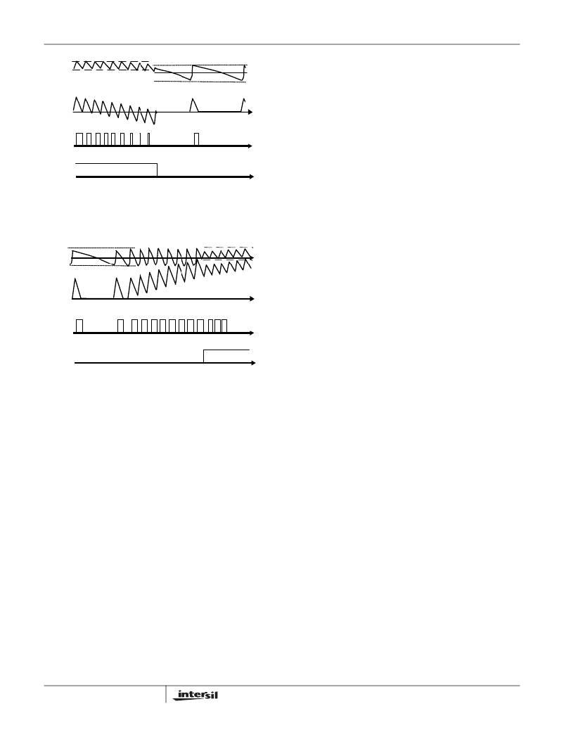
�FIGURE� 35.� CCM—HYSTERETIC� TRANSITION�
�voltage� for� regular� buck� operation,� which� means� the� current�
�is� freewheeling� through� lower� MOSFET.� For� the� second�
�channel� of� the� DDR� application,� the� phase� pin� voltage� needs�
�to� be� higher� than� 0.1V� to� activate� the� current� sensing� circuit�
�VOUT�
�t�
�for� bidirectional� current� sensing.� The� current� sampling�
�finishes� at� about� 400ns� after� the� lower� MOSFET� has� turned�
�on.� This� current� information� is� held� for� current� mode� control�
�and� overcurrent� protection.� The� current� sensing� pin� can�
�IIND�
�1�
�2� 3� 4� 5�
�6� 7�
�8�
�t�
�source� up� to� 260μA.� The� current� sense� resistor� and� OCSET�
�resistor� can� be� adjusted� simultaneously� for� the� same�
�PHASE�
�COMP�
�MODE�
�OF�
�OPERAT� ION�
�HYSTERETIC�
�PWM�
�t�
�t�
�overcurrent� protection� level,� however,� the� current� sensing�
�gain� will� be� changed� only� according� to� the� current� sense�
�resistor� value,� which� will� affect� the� current� feedback� loop�
�gain.� The� middle� point� of� the� Isen� current� can� be� at� 75μA,�
�but� it� can� be� tuned� up� and� down� to� fit� application� needs.�
�If� another� channel� is� switching� at� the� moment� the� current�
�sample� is� finishing,� it� could� cause� current� sensing� error� and�
�FIGURE� 36.� HYSTERETIC—CCM� TRANSITION�
�If� load� current� slowly� increases� or� decreases,� mode�
�transition� will� occur� naturally,� as� described� in� Figures� 35� and�
�36;� however,� if� there� is� an� instantaneous� load� current�
�phase� voltage� jitter.� In� the� design� stage,� the� duty� cycles� and�
�synchronization� have� to� be� analyzed� for� all� the� input� voltage�
�and� load� conditions� to� reduce� the� chance� of� current� sensing�
�error.� The� relationship� between� the� sampled� current� and�
�MOSFET� current� is� given� by� Equation� 5:�
�increase� resulting� in� a� large� output� voltage� drop� before� the�
�hysteretic� mode� controller� responds,� a� comparator� with�
�threshold� of� 20mV� below� the� reference� voltage� will� be�
�I� SEN� (� R� CS� +� 140� )� =� r� DS� (� ON� )� I� D�
�(EQ.� 5)�
�tripped,� and� the� chip� will� jump� into� the� forced� PWM� mode�
�immediately.� The� PWM� controller� will� process� the� load�
�transient� smoothly.�
�Once� the� PWM� controller� is� engaged,� eight� consecutive�
�switching� cycles� of� negative� inductor� current� are� required� to�
�transition� back� to� the� hysteretic� mode.� In� this� way,� chattering�
�between� the� two� modes� is� prevented.� Current� sinking� during�
�the� 8� PWM� switching� cycle� dumps� energy� to� input,�
�smoothing� output� voltage� load� step-down.�
�As� a� side� effect� to� this� design,� the� comparator� may� be�
�triggered� consistently� if� the� ESR� of� the� capacitor� is� so� big�
�that� the� output� ripple� voltage� exceeds� the� 20mV� window,�
�resulting� in� a� pure� PWM� pulse.�
�The� PWM� error� amplifier� is� put� in� clamped� voltage� during� the�
�hysteretic� mode.� The� output� voltage� through� the� VOUT� pin�
�16�
�Which� means� the� current� sensing� pin� will� source� current� to�
�make� the� voltage� drop� on� the� MOSFET� equal� to� the� voltage�
�generated� on� the� sensing� resistor,� plus� the� internal� resistor,�
�along� the� ISEN� pin� current� flowing� path.�
�Feedback� Loop� Compensation�
�Both� channel� PWM� controllers� have� internally� compensated�
�error� amplifiers.� To� make� internal� compensation� possible�
�several� design� measures� were� taken.�
�?� The� ramp� signal� applied� to� the� PWM� comparator� has� been�
�made� proportional� to� the� input� voltage� by� the� VIN� pin.� This�
�keeps� the� product� of� the� modulator� gain� and� the� input�
�voltage� constant� even� when� the� input� voltage� varies.�
�?� The� load� current� proportional� signal� is� derived� from� the�
�voltage� drop� across� the� lower� MOSFET� during� the� PWM�
�off� time� interval,� and� is� subtracted� from� the� error� amplifier�
�FN9094.7�
�May� 4,� 2009�
�相关PDF资料 |
PDF描述 |
|---|---|
| 80MXC5600MEFCSN35X40 | CAP ALUM 5600UF 80V 20% SNAP-IN |
| EL5126CLZ-T13 | IC VOLTAGE GEN 8CH TFT-LCD 32QFN |
| 250MXC1000MEFCSN35X35 | CAP ALUM 1000UF 250V 20% SNAP-IN |
| EL5126CLZ-T7 | IC VOLTAGE GEN 8CH TFT-LCD 32QFN |
| 400SXC330MEFCSN30X45 | CAP ALUM 330UF 400V 20% SNAP-IN |
相关代理商/技术参数 |
参数描述 |
|---|---|
| ISL6227IRZ-T | 功能描述:IC CONTROLLER DDR, DDR2 28QFN RoHS:是 类别:集成电路 (IC) >> PMIC - 稳压器 - 专用型 系列:- 标准包装:43 系列:- 应用:控制器,Intel VR11 输入电压:5 V ~ 12 V 输出数:1 输出电压:0.5 V ~ 1.6 V 工作温度:-40°C ~ 85°C 安装类型:表面贴装 封装/外壳:48-VFQFN 裸露焊盘 供应商设备封装:48-QFN(7x7) 包装:管件 |
| ISL6228 | 制造商:INTERSIL 制造商全称:Intersil Corporation 功能描述:High-Performance Dual-Output Buck Controller for Notebook Applications |
| ISL6228EVAL3Z | 功能描述:EVALUATION BOARD FOR ISL6228 RoHS:是 类别:编程器,开发系统 >> 评估板 - DC/DC 与 AC/DC(离线)SMPS 系列:Robust Ripple Regulator™ (R³) 产品培训模块:Obsolescence Mitigation Program 标准包装:1 系列:True Shutdown™ 主要目的:DC/DC,步升 输出及类型:1,非隔离 功率 - 输出:- 输出电压:- 电流 - 输出:1A 输入电压:2.5 V ~ 5.5 V 稳压器拓扑结构:升压 频率 - 开关:3MHz 板类型:完全填充 已供物品:板 已用 IC / 零件:MAX8969 |
| ISL6228HIEVAL3Z | 功能描述:EVALUATION BOARD FOR ISL6228HI RoHS:是 类别:编程器,开发系统 >> 评估板 - DC/DC 与 AC/DC(离线)SMPS 系列:Robust Ripple Regulator™ (R³) 产品培训模块:Obsolescence Mitigation Program 标准包装:1 系列:True Shutdown™ 主要目的:DC/DC,步升 输出及类型:1,非隔离 功率 - 输出:- 输出电压:- 电流 - 输出:1A 输入电压:2.5 V ~ 5.5 V 稳压器拓扑结构:升压 频率 - 开关:3MHz 板类型:完全填充 已供物品:板 已用 IC / 零件:MAX8969 |
| ISL6228HRTZ | 功能描述:IC REG CTRLR BUCK PWM 28-TQFN RoHS:是 类别:集成电路 (IC) >> PMIC - 稳压器 - DC DC 切换控制器 系列:Robust Ripple Regulator™ (R³) 产品培训模块:Lead (SnPb) Finish for COTS Obsolescence Mitigation Program 标准包装:2,500 系列:- PWM 型:电流模式 输出数:1 频率 - 最大:275kHz 占空比:50% 电源电压:18 V ~ 110 V 降压:无 升压:无 回扫:无 反相:无 倍增器:无 除法器:无 Cuk:无 隔离:是 工作温度:-40°C ~ 85°C 封装/外壳:8-SOIC(0.154",3.90mm 宽) 包装:带卷 (TR) |
发布紧急采购,3分钟左右您将得到回复。