参数资料
| 型号: | ISL62883IRTZ |
| 厂商: | Intersil |
| 文件页数: | 21/37页 |
| 文件大小: | 0K |
| 描述: | IC REG PWM 3PHASE BUCK 40TQFN |
| 标准包装: | 60 |
| 应用: | 控制器,Intel IMVP-6.5? |
| 输入电压: | 5 V ~ 21 V |
| 输出数: | 1 |
| 输出电压: | 0.013 V ~ 1.5 V |
| 工作温度: | -40°C ~ 100°C |
| 安装类型: | 表面贴装 |
| 封装/外壳: | 40-WFQFN 裸露焊盘 |
| 供应商设备封装: | 40-TQFN-EP(5x5) |
| 包装: | 管件 |
第1页第2页第3页第4页第5页第6页第7页第8页第9页第10页第11页第12页第13页第14页第15页第16页第17页第18页第19页第20页当前第21页第22页第23页第24页第25页第26页第27页第28页第29页第30页第31页第32页第33页第34页第35页第36页第37页
�� �
�
�ISL62883,� ISL62883B�
�ISUM+�
�Resistor� Current-Sensing� Network�
�Phase1� Phase2� Phase3�
�Rntcs�
�Cn.1�
�L�
�L�
�L�
�Rp�
�Cn.2� Vcn�
�Rntc�
�Rn�
�OPTIONAL�
�Ri�
�ISUM-�
�DCR�
�DCR�
�DCR�
�Rsum�
�Rsum�
�Rsum�
�ISUM+�
�Rip�
�Cip�
�Rsen�
�Rsen�
�Rsen�
�Ro�
�Vcn�
�Cn�
�Ri�
�ISUM-�
�V� Cn� (� s� )� =� ------------� � I� o� (� s� )� � A� Rsen� (� s� )�
�R� sen�
�N�
�A� Rsen� (� s� )� =� ----------------------�
�s�
�ω� sns�
�ω� Rsen� =� ---------------------------�
�R� sum�
�V� Cn� =� ?� -----------------------------------------� � ------------� ?� � I� o�
�R� sum�
�N�
�?� ?�
�OPTIONAL�
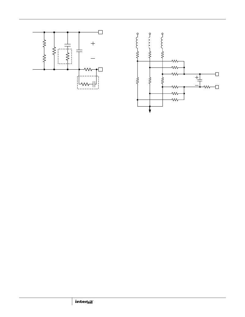
�FIGURE� 19.� OPTIONAL� CIRCUITS� FOR� RING� BACK� REDUCTION�
�Figure� 18� shows� the� output� voltage� ring� back� problem� during�
�load� transient� response.� The� load� current� i� o� has� a� fast� step�
�change,� but� the� inductor� current� i� L� cannot� accurately� follow.�
�Instead,� i� L� responds� in� first� order� system� fashion� due� to� the�
�nature� of� current� loop.� The� ESR� and� ESL� effect� of� the� output�
�capacitors� makes� the� output� voltage� V� o� dip� quickly� upon� load�
�current� change.� However,� the� controller� regulates� V� o� according� to�
�the� droop� current� i� droop� ,� which� is� a� real-time� representation� of� i� L� ;�
�therefore� it� pulls� V� o� back� to� the� level� dictated� by� i� L� ,� causing� the�
�ring� back� problem.� This� phenomenon� is� not� observed� when� the�
�output� capacitor� have� very� low� ESR� and� ESL,� such� as� all� ceramic�
�capacitors.�
�Figure� 19� shows� two� optional� circuits� for� reduction� of� the� ring�
�back.� R� ip� and� C� ip� form� an� R-C� branch� in� parallel� with� R� i� ,� providing�
�a� lower� impedance� path� than� R� i� at� the� beginning� of� i� o� change.�
�R� ip� and� C� ip� do� not� have� any� effect� at� steady� state.� Through�
�proper� selection� of� R� ip� and� C� ip� values,� i� droop� can� resemble� i� o�
�rather� than� i� L� ,� and� V� o� will� not� ring� back.� The� recommended� value�
�for� R� ip� is100� Ω� .� C� ip� should� be� determined� through� tuning� the� load�
�transient� response� waveforms� on� an� actual� board.� The�
�recommended� range� for� C� ip� is� 100pF~2000pF.�
�C� n� is� the� capacitor� used� to� match� the� inductor� time� constant.� It�
�usually� takes� the� parallel� of� two� (or� more)� capacitors� to� get� the�
�desired� value.� Figure� 19� shows� that� two� capacitors� C� n.1� and� C� n.2�
�are� in� parallel.� Resistor� R� n� is� an� optional� component� to� reduce�
�the� V� o� ring� back.� At� steady� state,� C� n.1� +C� n.2� provides� the� desired�
�C� n� capacitance.� At� the� beginning� of� i� o� change,� the� effective�
�capacitance� is� less� because� R� n� increases� the� impedance� of� the�
�C� n.1� branch.� As� explained� in� Figure� 16,� V� o� tends� to� dip� when� C� n� is�
�too� small,� and� this� effect� will� reduce� the� V� o� ring� back.� This� effect�
�is� more� pronounced� when� C� n.1� is� much� larger� than� C� n.2� .� It� is� also�
�more� pronounced� when� R� n� is� bigger.� However,� the� presence� of�
�R� n� increases� the� ripple� of� the� V� n� signal� if� C� n.2� is� too� small.� It� is�
�recommended� to� keep� C� n.2� greater� than� 2200pF.� R� n� value�
�usually� is� a� few� ohms.� C� n.1� ,� C� n.2� and� R� n� values� should� be�
�determined� through� tuning� the� load� transient� response�
�waveforms� on� an� actual� board.�
�21�
�Ro�
�Ro�
�Io�
�FIGURE� 20.� RESISTOR� CURRENT-SENSING� NETWORK�
�Figure� 20� shows� the� resistor� current-sensing� network� for� a�
�3-phase� solution.� Each� inductor� has� a� series� current-sensing�
�resistor� R� sen� .� R� sum� and� R� o� are� connected� to� the� R� sen� pads� to�
�accurately� capture� the� inductor� current� information.� The� R� sum�
�and� R� o� resistors� are� connected� to� capacitor� C� n� .� R� sum� and� C� n�
�form� a� a� filter� for� noise� attenuation.� Equations� 25� thru� 27� give�
�V� Cn� (s)� expression:�
�(EQ.� 25)�
�1�
�(EQ.� 26)�
�1� +� ------------�
�1�
�(EQ.� 27)�
�N�
�--------------� � C� n�
�Transfer� function� A� Rsen� (s)� always� has� unity� gain� at� DC.�
�Current-sensing� resistor� R� sen� value� will� not� have� significant�
�variation� over� temperature,� so� there� is� no� need� for� the� NTC�
�network.�
�The� recommended� values� are� R� sum� =� 1k� Ω� and� C� n� =� 5600pF.�
�Overcurrent� Protection�
�Refer� to� Equation� 1� and� Figures� 9,� 14� and� 20;� resistor� R� i� sets� the�
�droop� current� I� droop� .� Table� 3� shows� the� internal� OCP� threshold.� It�
�is� recommended� to� design� I� droop� without� using� the� R� comp�
�resistor.�
�For� example,� the� OCP� threshold� is� 60μA� for� 3-phase� solution.� We�
�will� design� I� droop� to� be� 38.8μA� at� full� load,� so� the� OCP� trip� level� is�
�1.55� times� of� the� full� load� current.�
�For� inductor� DCR� sensing,� Equation� 28� gives� the� DC� relationship�
�of� V� cn� (s)� and� I� o� (s).�
�?� ?�
�?� R� ntcnet� DCR� ?�
�(EQ.� 28)�
�N�
�?� R� ntcnet� +� --------------� ?�
�FN6891.4�
�June� 21,� 2011�
�相关PDF资料 |
PDF描述 |
|---|---|
| ISL6292BCRZ | IC CHARGER LI-ION 4.2V 4X4 16QFN |
| ISL6294IBZ | IC CHRGR LI-ION SGL 8-SOIC |
| ISL6306IRZ | IC REG CTRLR BUCK PWM VM 40-QFN |
| ISL6307AIRZ | IC REG CTRLR BUCK PWM VM 48-QFN |
| ISL6307BIRZ | IC REG CTRLR BUCK PWM VM 48-QFN |
相关代理商/技术参数 |
参数描述 |
|---|---|
| ISL62883IRTZ-T | 功能描述:直流/直流开关调节器 3 PHS PWM BUCKG FOR MICROPROC PWR SUP RoHS:否 制造商:International Rectifier 最大输入电压:21 V 开关频率:1.5 MHz 输出电压:0.5 V to 0.86 V 输出电流:4 A 输出端数量: 最大工作温度: 安装风格:SMD/SMT 封装 / 箱体:PQFN 4 x 5 |
| ISL62884C | 制造商:INTERSIL 制造商全称:Intersil Corporation 功能描述:Single-Phase PWM Regulator for IMVP-6a?¢ Mobile CPUs |
| ISL62884CEVAL2Z | 功能描述:EVAL BOARD FOR ISL62884C RoHS:是 类别:编程器,开发系统 >> 评估板 - DC/DC 与 AC/DC(离线)SMPS 系列:- 产品培训模块:Obsolescence Mitigation Program 标准包装:1 系列:True Shutdown™ 主要目的:DC/DC,步升 输出及类型:1,非隔离 功率 - 输出:- 输出电压:- 电流 - 输出:1A 输入电压:2.5 V ~ 5.5 V 稳压器拓扑结构:升压 频率 - 开关:3MHz 板类型:完全填充 已供物品:板 已用 IC / 零件:MAX8969 |
| ISL62884CHRTZ | 功能描述:直流/直流开关调节器 1-PHS PWM BUCKG FOR MICROPROC PWR SUPPLY RoHS:否 制造商:International Rectifier 最大输入电压:21 V 开关频率:1.5 MHz 输出电压:0.5 V to 0.86 V 输出电流:4 A 输出端数量: 最大工作温度: 安装风格:SMD/SMT 封装 / 箱体:PQFN 4 x 5 |
| ISL62884CHRTZ-T | 功能描述:直流/直流开关调节器 1-PHS PWM BUCKG FOR MICROPROC PWR SUPPLY RoHS:否 制造商:International Rectifier 最大输入电压:21 V 开关频率:1.5 MHz 输出电压:0.5 V to 0.86 V 输出电流:4 A 输出端数量: 最大工作温度: 安装风格:SMD/SMT 封装 / 箱体:PQFN 4 x 5 |
发布紧急采购,3分钟左右您将得到回复。