参数资料
| 型号: | ISL6313IRZ |
| 厂商: | Intersil |
| 文件页数: | 11/33页 |
| 文件大小: | 0K |
| 描述: | IC CTRLR PWM 2PHASE BUCK 36-QFN |
| 产品培训模块: | Solutions for Industrial Control Applications |
| 标准包装: | 50 |
| 应用: | 控制器,Intel VR11,AMD CPU |
| 输入电压: | 5 V ~ 12 V |
| 输出数: | 1 |
| 输出电压: | 0.5 V ~ 1.6 V |
| 工作温度: | -40°C ~ 85°C |
| 安装类型: | 表面贴装 |
| 封装/外壳: | 36-WFQFN 裸露焊盘 |
| 供应商设备封装: | 36-TQFN 裸露焊盘(6x6) |
| 包装: | 管件 |
第1页第2页第3页第4页第5页第6页第7页第8页第9页第10页当前第11页第12页第13页第14页第15页第16页第17页第18页第19页第20页第21页第22页第23页第24页第25页第26页第27页第28页第29页第30页第31页第32页第33页
�� �
�
�ISL6313�
�The� output� capacitors� conduct� the� ripple� component� of� the�
�inductor� current.� In� the� case� of� multi-phase� converters,� the�
�capacitor� current� is� the� sum� of� the� ripple� currents� from� each�
�of� the� individual� channels.� Compare� Equation� 1� to� the�
�expression� for� the� peak-to-peak� current� after� the� summation�
�of� N� symmetrically� phase-shifted� inductor� currents� in�
�Equation� 2.� Peak-to-peak� ripple� current� decreases� by� an�
�amount� proportional� to� the� number� of� channels.� Output�
�voltage� ripple� is� a� function� of� capacitance,� capacitor�
�equivalent� series� resistance� (ESR),� and� inductor� ripple�
�current.� Reducing� the� inductor� ripple� current� allows� the�
�designer� to� use� fewer� or� less� costly� output� capacitors.�
�which� a� PWM� signal� can� occur� is� generated� by� an� internal�
�clock,� whose� cycle� time� is� the� inverse� of� the� switching�
�frequency� set� by� the� resistor� connected� to� the� FS� pin.� The�
�advantage� of� Intersil’s� proprietary� Active� Pulse� Positioning�
�(APP)� modulator� is� that� the� PWM� signal� has� the� ability� to�
�turn� on� at� any� point� during� this� PWM� time� interval,� and� turn�
�off� immediately� after� the� PWM� signal� has� transitioned� high.�
�This� is� important� because� it� allows� the� controller� to� quickly�
�respond� to� output� voltage� drops� associated� with� current� load�
�spikes,� while� avoiding� the� ring� back� affects� associated� with�
�other� modulation� schemes.�
�The� PWM� output� state� is� driven� by� the� position� of� the� error�
�L� ?� f� S� ?� V�
�(� V� IN� –� N� ?� V� OUT� )� ?� V� OUT�
�I� C� (� P-P� )� =� --------------------------------------------------------------------�
�IN�
�(EQ.� 2)�
�amplifier� output� signal,� V� COMP� minus� the� current� correction�
�signal� relative� to� the� proprietary� modulator� ramp� waveform�
�Another� benefit� of� interleaving� is� to� reduce� input� ripple�
�current.� Input� capacitance� is� determined� in� part� by� the�
�maximum� input� ripple� current.� Multiphase� topologies� can�
�improve� overall� system� cost� and� size� by� lowering� input� ripple�
�current� and� allowing� the� designer� to� reduce� the� cost� of� input�
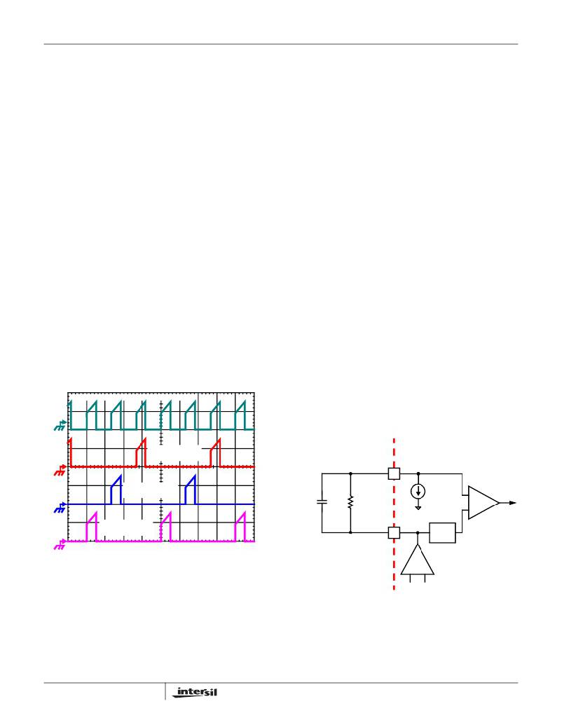
�capacitance.� The� example� in� Figure� 2� illustrates� input�
�currents� from� a� three-phase� converter� combining� to� reduce�
�the� total� input� ripple� current.�
�The� converter� depicted� in� Figure� 2� delivers� 1.5V� to� a� 36A� load�
�from� a� 12V� input.� The� RMS� input� capacitor� current� is� 5.9A.�
�Compare� this� to� a� single-phase� converter� also� stepping� down�
�12V� to� 1.5V� at� 36A.� The� single-phase� converter� has�
�11.9A� RMS� input� capacitor� current.� The� single-phase� converter�
�must� use� an� input� capacitor� bank� with� twice� the� RMS� current�
�capacity� as� the� equivalent� three-phase� converter.�
�INPUT-CAPACITOR CURRENT, 10A/DIV�
�as� illustrated� in� Figure� 4.� At� the� beginning� of� each� PWM� time�
�interval,� this� modified� V� COMP� signal� is� compared� to� the�
�internal� modulator� waveform.� As� long� as� the� modified�
�V� COMP� voltage� is� lower� then� the� modulator� waveform�
�voltage,� the� PWM� signal� is� commanded� low.� The� internal�
�MOSFET� driver� detects� the� low� state� of� the� PWM� signal� and�
�turns� off� the� upper� MOSFET� and� turns� on� the� lower�
�synchronous� MOSFET.� When� the� modified� V� COMP� voltage�
�crosses� the� modulator� ramp,� the� PWM� output� transitions�
�high,� turning� off� the� synchronous� MOSFET� and� turning� on�
�the� upper� MOSFET.� The� PWM� signal� will� remain� high� until�
�the� modified� V� COMP� voltage� crosses� the� modulator� ramp�
�again.� When� this� occurs� the� PWM� signal� will� transition� low�
�again.�
�During� each� PWM� time� interval� the� PWM� signal� can� only�
�transition� high� once.� Once� PWM� transitions� high� it� can� not�
�transition� high� again� until� the� beginning� of� the� next� PWM�
�time� interval.� This� prevents� the� occurrence� of� double� PWM�
�pulses� occurring� during� a� single� period.�
�CHANNEL� 3�
�INPUT� CURRENT�
�EXTERNAL� CIRCUIT�
�ISL6313� INTERNAL� CIRCUIT�
�APA�
�CHANNEL� 2�
�INPUT� CURRENT�
�CHANNEL� 1�
�INPUT� CURRENT�
�C� APA�
�R� APA�
�V� APA,TRIP�
�COMP�
�100μA�
�LOW�
�PASS�
�FILTER�
�+�
�-�
�APA�
�TO� APA�
�CIRCUITRY�
�1μs/DIV�
�FIGURE� 2.� CHANNEL� INPUT� CURRENTS� AND�
�INPUT-CAPACITOR� RMS� CURRENT� FOR�
�3-PHASE� CONVERTER�
�Active� Pulse� Positioning� (APP)� Modulated� PWM�
�Operation�
�The� ISL6313� uses� a� proprietary� Active� Pulse� Positioning�
�(APP)� modulation� scheme� to� control� the� internal� PWM�
�signals� that� command� each� channel’s� driver� to� turn� their�
�upper� and� lower� MOSFETs� on� and� off.� The� time� interval� in�
�11�
�ERROR�
�AMPLIFIER�
�FIGURE� 3.� ADAPTIVE� PHASE� ALIGNMENT� DETECTION�
�Adaptive� Phase� Alignment� (APA)�
�To� further� improve� the� transient� response,� the� ISL6313� also�
�implements� Intersil’s� proprietary� Adaptive� Phase� Alignment�
�(APA)� technique,� which� turns� on� all� of� the� channels� together�
�at� the� same� time� during� large� current� step� transient� events.�
�FN6448.2�
�September� 2,� 2008�
�相关PDF资料 |
PDF描述 |
|---|---|
| ISL6314IRZ | IC CTRLR PWM 1PHASE BUCK 32-QFN |
| ISL6315IRZ | IC REG CTRLR BUCK PWM VM 24-QFN |
| ISL6316IRZ | IC REG CTRLR BUCK PWM VM 40-QFN |
| ISL6322GIRZ-T | IC CTRLR PWM BUCK 48-QFN |
| ISL6322IRZ | IC CTRLR PWM 4PHASE BUCK 48-QFN |
相关代理商/技术参数 |
参数描述 |
|---|---|
| ISL6313IRZ-T | 功能描述:IC CTRLR PWM 2PHASE BUCK 36-QFN RoHS:是 类别:集成电路 (IC) >> PMIC - 稳压器 - 专用型 系列:- 标准包装:43 系列:- 应用:控制器,Intel VR11 输入电压:5 V ~ 12 V 输出数:1 输出电压:0.5 V ~ 1.6 V 工作温度:-40°C ~ 85°C 安装类型:表面贴装 封装/外壳:48-VFQFN 裸露焊盘 供应商设备封装:48-QFN(7x7) 包装:管件 |
| ISL6314CRZ | 功能描述:电压模式 PWM 控制器 1-PH PWM CNTRLR W/1 INTEGRTD DRVRS 32LD RoHS:否 制造商:Texas Instruments 输出端数量:1 拓扑结构:Buck 输出电压:34 V 输出电流: 开关频率: 工作电源电压:4.5 V to 5.5 V 电源电流:600 uA 最大工作温度:+ 125 C 最小工作温度:- 40 C 封装 / 箱体:WSON-8 封装:Reel |
| ISL6314CRZ-T | 功能描述:IC CTRLR PWM 1PHASE BUCK 32-QFN RoHS:是 类别:集成电路 (IC) >> PMIC - 稳压器 - 专用型 系列:- 标准包装:43 系列:- 应用:控制器,Intel VR11 输入电压:5 V ~ 12 V 输出数:1 输出电压:0.5 V ~ 1.6 V 工作温度:-40°C ~ 85°C 安装类型:表面贴装 封装/外壳:48-VFQFN 裸露焊盘 供应商设备封装:48-QFN(7x7) 包装:管件 |
| ISL6314CRZ-TR5453 | 制造商:Intersil Corporation 功能描述:STD. ISL6314CRZ-T W/GOLD BOND WIRE ONLY T&R - Tape and Reel |
| ISL6314CRZ-TS2568 | 制造商:Intersil Corporation 功能描述:- Tape and Reel |
发布紧急采购,3分钟左右您将得到回复。