参数资料
| 型号: | ISL6314IRZ-T |
| 厂商: | Intersil |
| 文件页数: | 29/32页 |
| 文件大小: | 0K |
| 描述: | IC CTRLR PWM 1PHASE BUCK 32-QFN |
| 产品培训模块: | Solutions for Industrial Control Applications |
| 标准包装: | 6,000 |
| 应用: | 控制器,Intel VR11,AMD CPU |
| 输入电压: | 5 V ~ 12 V |
| 输出数: | 1 |
| 输出电压: | 0.38 V ~ 1.6 V |
| 工作温度: | -40°C ~ 85°C |
| 安装类型: | 表面贴装 |
| 封装/外壳: | 32-VFQFN 裸露焊盘 |
| 供应商设备封装: | 32-QFN 裸露焊盘(5x5) |
| 包装: | 带卷 (TR) |
第1页第2页第3页第4页第5页第6页第7页第8页第9页第10页第11页第12页第13页第14页第15页第16页第17页第18页第19页第20页第21页第22页第23页第24页第25页第26页第27页第28页当前第29页第30页第31页第32页
�� �
�
�ISL6314�
�addresses� the� leading� edge.� Normally,� the� trailing� edge�
�dictates� the� selection� of� L� because� duty� cycles� are� usually�
�less� than� 50%.� Nevertheless,� both� inequalities� should� be�
�evaluated,� and� L� should� be� selected� based� on� the� lower� of�
�the� two� results.� In� each� equation,� L� is� the� inductance,� and� C�
�is� the� total� output� capacitance.�
�current� rating� which� will� minimize� the� total� number� of� input�
�capacitors� required� to� support� the� RMS� current� calculated.�
�The� voltage� rating� of� the� capacitors� should� also� be� at� least�
�1.25x� greater� than� the� maximum� input� voltage.�
�.�
�0.6�
�L� ≤� -------------------------� ?� Δ� V� MAX� –� (� Δ� I� ?� ESR� )�
�2� ?� C� ?� V� O�
�(� Δ� I� )� 2�
�(EQ.� 40)�
�L� ≤� --------------------� ?� Δ� V� MAX� –� (� Δ� I� ?� ESR� )� ?� ?� V� IN� –� V� O� ?�
�(� Δ� I� )� 2�
�1.25� ?� C�
�Switching� Frequency�
�?� ?�
�(EQ.� 41)�
�0.4�
�There� are� a� number� of� variables� to� consider� when� choosing�
�the� switching� frequency,� as� there� are� considerable� effects� on�
�the� upper� MOSFET� loss� calculation.� These� effects� are�
�outlined� in� “MOSFETs”� on� page� 23,� and� they� establish� the�
�upper� limit� for� the� switching� frequency.� The� lower� limit� is�
�0.2�
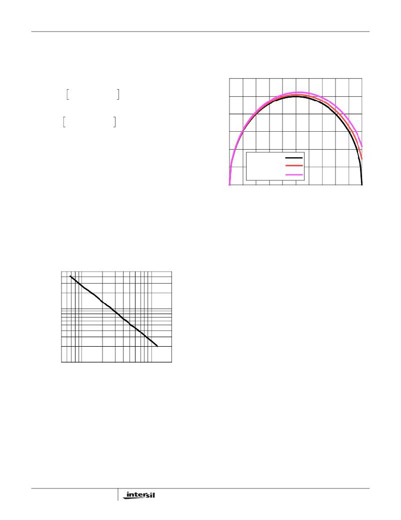
�I� L(P-P)� =� 0�
�I� L(P-P)� =� 0.5� I� O�
�I� L(P-P)� =� 0.75� I� O�
�established� by� the� requirement� for� fast� transient� response�
�0�
�0�
�0.2�
�0.4�
�0.6�
�0.8�
�1.0�
�and� small� output-voltage� ripple.� Choose� the� lowest� switching�
�frequency� that� allows� the� regulator� to� meet� the�
�transient-response� requirements.�
�Switching� frequency� is� determined� by� the� selection� of� the�
�frequency-setting� resistor,� R� T� .� Figure� 22� and� Equation� 42�
�are� provided� to� assist� in� selecting� the� correct� value� for� R� T� .�
�DUTY� CYCLE� (V� O� /V� IN� )�
�FIGURE� 23.� NORMALIZED� INPUT-CAPACITOR� RMS�
�CURRENT� FOR� SINGLE-PHASE� CONVERTER�
�Low� capacitance,� high-frequency� ceramic� capacitors� are�
�needed� in� addition� to� the� input� bulk� capacitors� to� suppress�
�leading� and� falling� edge� voltage� spikes.� The� spikes� result� from�
�R� T� =� 10�
�[� 10.61� –� (� 1.035� ?� log� (� f� S� )� )� ]�
�(EQ.� 42)�
�the� high� current� slew� rate� produced� by� the� upper� MOSFET�
�turn� on� and� off.� Select� low� ESL� ceramic� capacitors� and� place�
�one� as� close� as� possible� to� each� upper� MOSFET� drain� to�
�500�
�100�
�minimize� board� parasitics� and� maximize� suppression.�
�Layout� Considerations�
�MOSFETs� switch� very� fast� and� efficiently.� The� speed� with�
�which� the� current� transitions� from� one� device� to� another�
�causes� voltage� spikes� across� the� interconnecting�
�impedances� and� parasitic� circuit� elements.� These� voltage�
�spikes� can� degrade� efficiency,� radiate� noise� into� the� circuit�
�and� lead� to� device� overvoltage� stress.� Careful� component�
�selection,� layout,� and� placement� minimizes� these� voltage�
�spikes.� Consider,� as� an� example,� the� turnoff� transition� of� the�
�upper� PWM� MOSFET.� Prior� to� turn-off,� the� upper� MOSFET�
�10�
�50� 100� 1k�
�SWITCHING� FREQUENCY� (kHz)�
�FIGURE� 22.� R� T� vs� SWITCHING� FREQUENCY�
�2k�
�was� carrying� channel� current.� During� the� turn-off,� current�
�stops� flowing� in� the� upper� MOSFET� and� is� picked� up� by� the�
�lower� MOSFET.� Any� inductance� in� the� switched� current� path�
�generates� a� large� voltage� spike� during� the� switching� interval.�
�Input� Capacitor� Selection�
�The� input� capacitors� are� responsible� for� sourcing� the� AC�
�component� of� the� input� current� flowing� into� the� upper�
�MOSFETs.� Their� RMS� current� capacity� must� be� sufficient� to�
�handle� the� ac� component� of� the� current� drawn� by� the� upper�
�MOSFETs� which� is� related� to� duty� cycle� and� the� number� of�
�active� phases.�
�Use� Figure� 23� to� determine� the� input-capacitor� RMS� current�
�requirement� set� by� the� duty� cycle,� maximum� sustained�
�output� current� (I� O� ),� and� the� ratio� of� the� peak-to-peak� inductor�
�current� (I� L(P-P)� )� to� I� O� .� Select� a� bulk� capacitor� with� a� ripple�
�29�
�Careful� component� selection,� tight� layout� of� the� critical�
�components,� and� short,� wide� circuit� traces� minimize� the�
�magnitude� of� voltage� spikes.�
�There� are� two� sets� of� critical� components� in� a� DC/DC�
�converter� using� a� ISL6314� controller.� The� power�
�components� are� the� most� critical� because� they� switch� large�
�amounts� of� energy.� Next,� are� small� signal� components� that�
�connect� to� sensitive� nodes� or� supply� critical� bypassing�
�current� and� signal� coupling.�
�FN6455.2�
�October� 8,� 2009�
�相关PDF资料 |
PDF描述 |
|---|---|
| ESM24DRYI-S13 | CONN EDGECARD 48POS .156 EXTEND |
| 1944-06M | COIL RF .27UH MOLDED UNSHIELDED |
| ISL95870HRUZ-T | IC CTRLR PWM 1PHASE GPU 16UTQFN |
| MIC5301-2.85YML TR | IC REG LDO 2.85V .15A 6-MLF |
| ISL95870AHRUZ-T | IC CTRLR PWM 1PHASE GPU 20UTQFN |
相关代理商/技术参数 |
参数描述 |
|---|---|
| ISL6315CRZ | 功能描述:IC REG CTRLR BUCK PWM VM 24-QFN RoHS:是 类别:集成电路 (IC) >> PMIC - 稳压器 - DC DC 切换控制器 系列:- 产品培训模块:Lead (SnPb) Finish for COTS Obsolescence Mitigation Program 标准包装:2,500 系列:- PWM 型:电流模式 输出数:1 频率 - 最大:275kHz 占空比:50% 电源电压:18 V ~ 110 V 降压:无 升压:无 回扫:无 反相:无 倍增器:无 除法器:无 Cuk:无 隔离:是 工作温度:-40°C ~ 85°C 封装/外壳:8-SOIC(0.154",3.90mm 宽) 包装:带卷 (TR) |
| ISL6315CRZ-T | 功能描述:IC REG CTRLR BUCK PWM VM 24-QFN RoHS:是 类别:集成电路 (IC) >> PMIC - 稳压器 - DC DC 切换控制器 系列:- 产品培训模块:Lead (SnPb) Finish for COTS Obsolescence Mitigation Program 标准包装:2,500 系列:- PWM 型:电流模式 输出数:1 频率 - 最大:275kHz 占空比:50% 电源电压:18 V ~ 110 V 降压:无 升压:无 回扫:无 反相:无 倍增器:无 除法器:无 Cuk:无 隔离:是 工作温度:-40°C ~ 85°C 封装/外壳:8-SOIC(0.154",3.90mm 宽) 包装:带卷 (TR) |
| ISL6315CRZ-TK | 功能描述:IC REG CTRLR BUCK PWM VM 24-QFN RoHS:是 类别:集成电路 (IC) >> PMIC - 稳压器 - DC DC 切换控制器 系列:- 产品培训模块:Lead (SnPb) Finish for COTS Obsolescence Mitigation Program 标准包装:2,500 系列:- PWM 型:电流模式 输出数:1 频率 - 最大:275kHz 占空比:50% 电源电压:18 V ~ 110 V 降压:无 升压:无 回扫:无 反相:无 倍增器:无 除法器:无 Cuk:无 隔离:是 工作温度:-40°C ~ 85°C 封装/外壳:8-SOIC(0.154",3.90mm 宽) 包装:带卷 (TR) |
| ISL6315IRZ | 功能描述:IC REG CTRLR BUCK PWM VM 24-QFN RoHS:是 类别:集成电路 (IC) >> PMIC - 稳压器 - DC DC 切换控制器 系列:- 产品培训模块:Lead (SnPb) Finish for COTS Obsolescence Mitigation Program 标准包装:2,500 系列:- PWM 型:电流模式 输出数:1 频率 - 最大:275kHz 占空比:50% 电源电压:18 V ~ 110 V 降压:无 升压:无 回扫:无 反相:无 倍增器:无 除法器:无 Cuk:无 隔离:是 工作温度:-40°C ~ 85°C 封装/外壳:8-SOIC(0.154",3.90mm 宽) 包装:带卷 (TR) |
| ISL6315IRZ-T | 功能描述:IC REG CTRLR BUCK PWM VM 24-QFN RoHS:是 类别:集成电路 (IC) >> PMIC - 稳压器 - DC DC 切换控制器 系列:- 产品培训模块:Lead (SnPb) Finish for COTS Obsolescence Mitigation Program 标准包装:2,500 系列:- PWM 型:电流模式 输出数:1 频率 - 最大:275kHz 占空比:50% 电源电压:18 V ~ 110 V 降压:无 升压:无 回扫:无 反相:无 倍增器:无 除法器:无 Cuk:无 隔离:是 工作温度:-40°C ~ 85°C 封装/外壳:8-SOIC(0.154",3.90mm 宽) 包装:带卷 (TR) |
发布紧急采购,3分钟左右您将得到回复。