参数资料
| 型号: | ISL6327AIRZ |
| 厂商: | Intersil |
| 文件页数: | 23/29页 |
| 文件大小: | 0K |
| 描述: | IC REG CTRLR BUCK PWM 48-QFN |
| 标准包装: | 43 |
| PWM 型: | 控制器 |
| 输出数: | 6 |
| 频率 - 最大: | 1MHz |
| 电源电压: | 4.75 V ~ 5.25 V |
| 降压: | 是 |
| 升压: | 无 |
| 回扫: | 无 |
| 反相: | 无 |
| 倍增器: | 无 |
| 除法器: | 无 |
| Cuk: | 无 |
| 隔离: | 无 |
| 工作温度: | -40°C ~ 85°C |
| 封装/外壳: | 48-VFQFN 裸露焊盘 |
| 包装: | 管件 |
第1页第2页第3页第4页第5页第6页第7页第8页第9页第10页第11页第12页第13页第14页第15页第16页第17页第18页第19页第20页第21页第22页当前第23页第24页第25页第26页第27页第28页第29页
�� �
�
�ISL6327A�
�.�
�ISL6327A�
�require� heat� sinks� and� forced� air� to� cool� the� MOSFETs,�
�inductors,� and� heat-dissipating� surfaces.�
�°C�
�COMP�
�IDROOP�
�INTERNAL�
�CIRCUIT�
�MOSFETS�
�The� choice� of� MOSFETs� depends� on� the� current� each�
�MOSFET� will� be� required� to� conduct;� the� switching�
�frequency;� the� capability� of� the� MOSFETs� to� dissipate� heat;�
�and� the� availability� and� nature� of� heat� sinking� and� air� flow.�
�FB�
�LOWER� MOSFET� POWER� CALCULATION�
�The� calculation� for� heat� dissipated� in� the� lower� MOSFET� is�
�VDIFF�
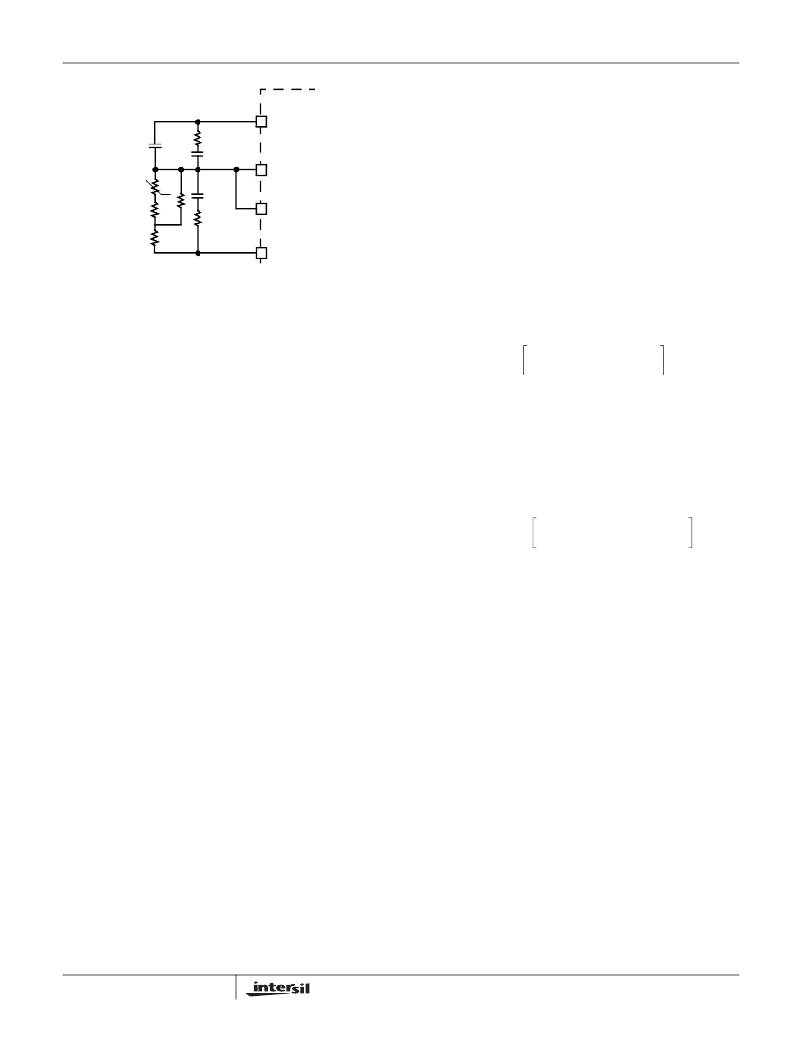
�FIGURE� 16.� EXTERNAL� TEMPERATURE� COMPENSATION�
�The� sensed� current� will� flow� out� of� IDROOP� pin� and� develop�
�the� droop� voltage� across� the� resistor� (R� FB� )� between� FB� and�
�VDIFF� pins.� If� R� FB� resistance� reduces� as� the� temperature�
�simple,� since� virtually� all� of� the� heat� loss� in� the� lower�
�MOSFET� is� due� to� current� conducted� through� the� channel�
�resistance� (r� DS(ON)� ).� In� Equation� 22,� I� M� is� the� maximum�
�continuous� output� current;� I� P-P� is� the� peak-to-peak� inductor�
�current� (see� Equation� 1);� d� is� the� duty� cycle� (V� OUT� /V� IN� );� and�
�L� is� the� per-channel� inductance.�
�?� I� M� ?� 2� I� L� (� P-P� )� 2� (� 1� –� d� )�
�P� LOW� ,� 1� =� r� DS� (� ON� )� ?� ------� ?� (� 1� –� d� )� +� ------------------------------------�
�increases,� the� temperature� impact� on� the� droop� can� be�
�compensated.� An� NTC� resistor� can� be� placed� close� to� the�
�power� stage� and� used� to� form� R� FB� .� Due� to� the� non-linear�
�temperature� characteristics� of� the� NTC,� a� resistor� network� is�
�?� N� ?� 12�
�(EQ.� 22)�
�needed� to� make� the� equivalent� resistance� between� FB� and�
�VDIFF� pin� reverse� proportional� to� the� temperature.�
�The� external� temperature� compensation� network� can� only�
�compensate� the� temperature� impact� on� the� droop,� while� it�
�has� no� impact� to� the� sensed� current� inside� ISL6327A.�
�Therefore,� this� network� cannot� compensate� for� the�
�An� additional� term� can� be� added� to� the� lower-MOSFET� loss�
�equation� to� account� for� additional� loss� accrued� during� the� dead�
�time� when� inductor� current� is� flowing� through� the� lower�
�MOSFET� body� diode.� This� term� is� dependent� on� the� diode�
�forward� voltage� at� I� M� ,� V� D(ON)� ;� the� switching� frequency,� f� S� ;� and�
�the� length� of� dead� times,� t� d1� and� t� d2� ,� at� the� beginning� and� the�
�end� of� the� lower-MOSFET� conduction� interval� respectively.�
�temperature� impact� on� the� overcurrent� protection� function.�
�.�
�I� P-P� ?�
�?� I�
�P� LOW� ,� 2� =� V� D� (� ON� )� f� S� ?� ------� +� I� ----------� ?� t�
�?� d1� +� ?� ?� ------� –� ----------� ?� ?� d2�
�I� M� P-P� M�
�?� N�
�General� Design� Guide�
�2� N� 2�
�t�
�(EQ.� 23)�
�This� design� guide� is� intended� to� provide� a� high-level�
�explanation� of� the� steps� necessary� to� create� a� multiphase�
�power� converter.� It� is� assumed� that� the� reader� is� familiar� with�
�many� of� the� basic� skills� and� techniques� referenced� below.� In�
�addition� to� this� guide,� Intersil� provides� complete� reference�
�designs� that� include� schematics,� bills� of� materials,� and�
�example� board� layouts� for� all� common� microprocessor�
�applications.�
�Power� Stages�
�The� first� step� in� designing� a� multiphase� converter� is� to�
�determine� the� number� of� phases.� This� determination�
�depends� heavily� on� the� cost� analysis� which� in� turn� depends�
�on� system� constraints� that� differ� from� one� design� to� the� next.�
�Principally,� the� designer� will� be� concerned� with� whether�
�components� can� be� mounted� on� both� sides� of� the� circuit�
�board;� whether� through-hole� components� are� permitted;� and�
�the� total� board� space� available� for� power-supply� circuitry.�
�Generally� speaking,� the� most� economical� solutions� are�
�those� in� which� each� phase� handles� between� 15A� and� 20A.�
�All� surface-mount� designs� will� tend� toward� the� lower� end� of�
�this� current� range.� If� through-hole� MOSFETs� and� inductors�
�can� be� used,� higher� per-phase� currents� are� possible.� In�
�Thus,� the� total� maximum� power� dissipated� in� each� lower�
�MOSFET� is� approximated� by� the� summation� of� P� LOW,1� and�
�P� LOW,2� .�
�UPPER� MOSFET� POWER� CALCULATION�
�In� addition� to� r� DS(ON)� losses,� a� large� portion� of� the� upper�
�MOSFET� losses� are� due� to� currents� conducted� across� the�
�input� voltage� (V� IN� )� during� switching.� Since� a� substantially�
�higher� portion� of� the� upper-MOSFET� losses� are� dependent� on�
�switching� frequency,� the� power� calculation� is� more� complex.�
�Upper� MOSFET� losses� can� be� divided� into� separate�
�components� involving� the� upper-MOSFET� switching� times;�
�the� lower-MOSFET� body-diode� reverse-recovery� charge,� Q� rr� ,�
�and� the� upper� MOSFET� r� DS(ON)� conduction� loss.�
�When� the� upper� MOSFET� turns� off,� the� lower� MOSFET� does�
�not� conduct� any� portion� of� the� inductor� current� until� the�
�voltage� at� the� phase� node� falls� below� ground.� Once� the�
�lower� MOSFET� begins� conducting,� the� current� in� the� upper�
�MOSFET� falls� to� zero� as� the� current� in� the� lower� MOSFET�
�ramps� up� to� assume� the� full� inductor� current.� In� Equation� 24,�
�the� required� time� for� this� commutation� is� t� 1� and� the�
�approximated� associated� power� loss� is� P� UP,1� .�
�P� UP� ,� 1� ≈� V� IN� ?� ------� +� ----------� ?� ?� ----� 1� ?� f� S�
�cases� where� board� space� is� the� limiting� constraint,� current�
�can� be� pushed� as� high� as� 40A� per� phase,� but� these� designs�
�23�
�?� N� 2� ?� ?� 2� ?�
�I� M� I� P-P� ?� t� ?�
�(EQ.� 24)�
�FN6833.0�
�February� 17,� 2009�
�相关PDF资料 |
PDF描述 |
|---|---|
| ISL6327IRZ | IC REG CTRLR BUCK PWM 48-QFN |
| ISL6328AIRZ | IC VOLTAGE REGULATOR |
| ISL6328IRZ | IC CTRLR PWM SYNC BUCK DL 48QFN |
| ISL6329IRZ-T | IC CTRLR PWM SYNC BUCK DL 60QFN |
| ISL6333IRZ | IC CTRLR PWM 3PHASE BUCK 48-QFN |
相关代理商/技术参数 |
参数描述 |
|---|---|
| ISL6327AIRZ-T | 功能描述:IC REG CTRLR BUCK PWM 48-QFN RoHS:是 类别:集成电路 (IC) >> PMIC - 稳压器 - DC DC 切换控制器 系列:- 产品培训模块:Lead (SnPb) Finish for COTS Obsolescence Mitigation Program 标准包装:2,500 系列:- PWM 型:电流模式 输出数:1 频率 - 最大:275kHz 占空比:50% 电源电压:18 V ~ 110 V 降压:无 升压:无 回扫:无 反相:无 倍增器:无 除法器:无 Cuk:无 隔离:是 工作温度:-40°C ~ 85°C 封装/外壳:8-SOIC(0.154",3.90mm 宽) 包装:带卷 (TR) |
| ISL6327CRZ | 功能描述:IC REG CTRLR BUCK PWM 48-QFN RoHS:是 类别:集成电路 (IC) >> PMIC - 稳压器 - DC DC 切换控制器 系列:- 产品培训模块:Lead (SnPb) Finish for COTS Obsolescence Mitigation Program 标准包装:2,500 系列:- PWM 型:电流模式 输出数:1 频率 - 最大:275kHz 占空比:50% 电源电压:18 V ~ 110 V 降压:无 升压:无 回扫:无 反相:无 倍增器:无 除法器:无 Cuk:无 隔离:是 工作温度:-40°C ~ 85°C 封装/外壳:8-SOIC(0.154",3.90mm 宽) 包装:带卷 (TR) |
| ISL6327CRZ-T | 功能描述:IC REG CTRLR BUCK PWM 48-QFN RoHS:是 类别:集成电路 (IC) >> PMIC - 稳压器 - DC DC 切换控制器 系列:- 产品培训模块:Lead (SnPb) Finish for COTS Obsolescence Mitigation Program 标准包装:2,500 系列:- PWM 型:电流模式 输出数:1 频率 - 最大:275kHz 占空比:50% 电源电压:18 V ~ 110 V 降压:无 升压:无 回扫:无 反相:无 倍增器:无 除法器:无 Cuk:无 隔离:是 工作温度:-40°C ~ 85°C 封装/外壳:8-SOIC(0.154",3.90mm 宽) 包装:带卷 (TR) |
| ISL6327IRZ | 功能描述:IC REG CTRLR BUCK PWM 48-QFN RoHS:是 类别:集成电路 (IC) >> PMIC - 稳压器 - DC DC 切换控制器 系列:- 产品培训模块:Lead (SnPb) Finish for COTS Obsolescence Mitigation Program 标准包装:2,500 系列:- PWM 型:电流模式 输出数:1 频率 - 最大:275kHz 占空比:50% 电源电压:18 V ~ 110 V 降压:无 升压:无 回扫:无 反相:无 倍增器:无 除法器:无 Cuk:无 隔离:是 工作温度:-40°C ~ 85°C 封装/外壳:8-SOIC(0.154",3.90mm 宽) 包装:带卷 (TR) |
| ISL6327IRZ-T | 功能描述:IC REG CTRLR BUCK PWM 48-QFN RoHS:是 类别:集成电路 (IC) >> PMIC - 稳压器 - DC DC 切换控制器 系列:- 产品培训模块:Lead (SnPb) Finish for COTS Obsolescence Mitigation Program 标准包装:2,500 系列:- PWM 型:电流模式 输出数:1 频率 - 最大:275kHz 占空比:50% 电源电压:18 V ~ 110 V 降压:无 升压:无 回扫:无 反相:无 倍增器:无 除法器:无 Cuk:无 隔离:是 工作温度:-40°C ~ 85°C 封装/外壳:8-SOIC(0.154",3.90mm 宽) 包装:带卷 (TR) |
发布紧急采购,3分钟左右您将得到回复。