参数资料
| 型号: | ISL6327AIRZ |
| 厂商: | Intersil |
| 文件页数: | 28/29页 |
| 文件大小: | 0K |
| 描述: | IC REG CTRLR BUCK PWM 48-QFN |
| 标准包装: | 43 |
| PWM 型: | 控制器 |
| 输出数: | 6 |
| 频率 - 最大: | 1MHz |
| 电源电压: | 4.75 V ~ 5.25 V |
| 降压: | 是 |
| 升压: | 无 |
| 回扫: | 无 |
| 反相: | 无 |
| 倍增器: | 无 |
| 除法器: | 无 |
| Cuk: | 无 |
| 隔离: | 无 |
| 工作温度: | -40°C ~ 85°C |
| 封装/外壳: | 48-VFQFN 裸露焊盘 |
| 包装: | 管件 |
第1页第2页第3页第4页第5页第6页第7页第8页第9页第10页第11页第12页第13页第14页第15页第16页第17页第18页第19页第20页第21页第22页第23页第24页第25页第26页第27页当前第28页第29页
�� �
�
�ISL6327A�
�when� output� current� is� increased� and� additional� phases� are�
�added� to� keep� the� component� cost� down� relative� to� the�
�single� phase� approach.�
�.�
�Component� Placement�
�Within� the� allotted� implementation� area,� orient� the� switching�
�components� first.� The� switching� components� are� the� most�
�critical� because� they� carry� large� amounts� of� energy� and� tend�
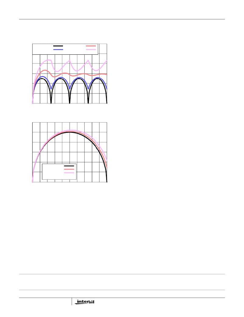
�0.3�
�I� L(P-P)� =� 0�
�I� L(P-P)� =� 0.25� I� O�
�I� L(P-P)� =� 0.5� I� O�
�I� L(P-P)� =� 0.75� I� O�
�to� generate� high� levels� of� noise.� Switching� component�
�placement� should� take� into� account� power� dissipation.� Align�
�the� output� inductors� and� MOSFETs� such� that� spaces�
�between� the� components� are� minimized� while� creating� the�
�0.2�
�0.1�
�PHASE� plane.� Place� the� Intersil� MOSFET� driver� IC� as� close�
�as� possible� to� the� MOSFETs� they� control� to� reduce� the�
�parasitic� impedances� due� to� trace� length� between� critical�
�driver� input� and� output� signals.� If� possible,� duplicate� the�
�same� placement� of� these� components� for� each� phase.�
�Next,� place� the� input� and� output� capacitors.� Position� one�
�high-frequency� ceramic� input� capacitor� next� to� each� upper�
�0�
�0�
�0.2�
�0.4�
�0.6�
�0.8�
�1.0�
�MOSFET� drain.� Place� the� bulk� input� capacitors� as� close� to� the�
�upper� MOSFET� drains� as� dictated� by� the� component� size� and�
�DUTY� CYCLE� (V� O/� V� IN� )�
�FIGURE� 21.� NORMALIZED� INPUT-CAPACITOR� RMS� CURRENT�
�vs� DUTY� CYCLE� FOR� 4-PHASE� CONVERTER�
�0.6�
�0.4�
�0.2�
�I� L(P-P)� =� 0�
�I� L(P-P)� =� 0.5� I� O�
�I� L(P-P)� =� 0.75� I� O�
�dimensions.� Long� distances� between� input� capacitors� and�
�MOSFET� drains� result� in� too� much� trace� inductance� and� a�
�reduction� in� capacitor� performance.� Locate� the� output�
�capacitors� between� the� inductors� and� the� load,� while� keeping�
�them� in� close� proximity� to� the� microprocessor� socket.�
�The� ISL6327A� can� be� placed� off� to� one� side� or� centered�
�relative� to� the� individual� phase� switching� components.�
�Routing� of� sense� lines� and� PWM� signals� will� guide� final�
�placement.� Critical� small� signal� components� to� place� close�
�to� the� controller� include� the� ISEN� resistors,� R� T� resistor,�
�feedback� resistor,� and� compensation� components.�
�Bypass� capacitors� for� the� ISL6327A� and� ISL66xx� driver� bias�
�supplies� must� be� placed� next� to� their� respective� pins.� Trace�
�parasitic� impedances� will� reduce� their� effectiveness.�
�0�
�0� 0.2� 0.4� 0.6� 0.8�
�DUTY� CYCLE� (V� O/� V� IN� )�
�FIGURE� 22.� NORMALIZED� INPUT-CAPACITOR� RMS�
�1.0�
�Plane� Allocation� and� Routing�
�Dedicate� one� solid� layer,� usually� a� middle� layer,� for� a� ground�
�CURRENT� vs� DUTY� CYCLE� FOR� SINGLE-PHASE�
�CONVERTER�
�Layout� Considerations�
�The� following� layout� strategies� are� intended� to� minimize� the�
�impact� of� board� parasitic� impedances� on� converter�
�performance� and� to� optimize� the� heat-dissipating� capabilities�
�of� the� printed-circuit� board.� These� sections� highlight� some�
�important� practices� which� should� not� be� overlooked� during� the�
�layout� process.�
�plane.� Make� all� critical� component� ground� connections� with�
�vias� to� this� plane.� Dedicate� one� additional� layer� for� power�
�planes;� breaking� the� plane� up� into� smaller� islands� of�
�common� voltage.� Use� the� remaining� layers� for� signal� wiring.�
�Route� phase� planes� of� copper� filled� polygons� on� the� top� and�
�bottom� once� the� switching� component� placement� is� set.� Size�
�the� trace� width� between� the� driver� gate� pins� and� the�
�MOSFET� gates� to� carry� 4A� of� current.� When� routing�
�components� in� the� switching� path,� use� short� wide� traces� to�
�reduce� the� associated� parasitic� impedances.�
�All� Intersil� U.S.� products� are� manufactured,� assembled� and� tested� utilizing� ISO9000� quality� systems.�
�Intersil� Corporation’s� quality� certifications� can� be� viewed� at� www.intersil.com/design/quality�
�Intersil� products� are� sold� by� description� only.� Intersil� Corporation� reserves� the� right� to� make� changes� in� circuit� design,� software� and/or� specifications� at� any� time� without�
�notice.� Accordingly,� the� reader� is� cautioned� to� verify� that� data� sheets� are� current� before� placing� orders.� Information� furnished� by� Intersil� is� believed� to� be� accurate� and�
�reliable.� However,� no� responsibility� is� assumed� by� Intersil� or� its� subsidiaries� for� its� use;� nor� for� any� infringements� of� patents� or� other� rights� of� third� parties� which� may� result�
�from� its� use.� No� license� is� granted� by� implication� or� otherwise� under� any� patent� or� patent� rights� of� Intersil� or� its� subsidiaries.�
�For� information� regarding� Intersil� Corporation� and� its� products,� see� www.intersil.com�
�28�
�FN6833.0�
�February� 17,� 2009�
�相关PDF资料 |
PDF描述 |
|---|---|
| ISL6327IRZ | IC REG CTRLR BUCK PWM 48-QFN |
| ISL6328AIRZ | IC VOLTAGE REGULATOR |
| ISL6328IRZ | IC CTRLR PWM SYNC BUCK DL 48QFN |
| ISL6329IRZ-T | IC CTRLR PWM SYNC BUCK DL 60QFN |
| ISL6333IRZ | IC CTRLR PWM 3PHASE BUCK 48-QFN |
相关代理商/技术参数 |
参数描述 |
|---|---|
| ISL6327AIRZ-T | 功能描述:IC REG CTRLR BUCK PWM 48-QFN RoHS:是 类别:集成电路 (IC) >> PMIC - 稳压器 - DC DC 切换控制器 系列:- 产品培训模块:Lead (SnPb) Finish for COTS Obsolescence Mitigation Program 标准包装:2,500 系列:- PWM 型:电流模式 输出数:1 频率 - 最大:275kHz 占空比:50% 电源电压:18 V ~ 110 V 降压:无 升压:无 回扫:无 反相:无 倍增器:无 除法器:无 Cuk:无 隔离:是 工作温度:-40°C ~ 85°C 封装/外壳:8-SOIC(0.154",3.90mm 宽) 包装:带卷 (TR) |
| ISL6327CRZ | 功能描述:IC REG CTRLR BUCK PWM 48-QFN RoHS:是 类别:集成电路 (IC) >> PMIC - 稳压器 - DC DC 切换控制器 系列:- 产品培训模块:Lead (SnPb) Finish for COTS Obsolescence Mitigation Program 标准包装:2,500 系列:- PWM 型:电流模式 输出数:1 频率 - 最大:275kHz 占空比:50% 电源电压:18 V ~ 110 V 降压:无 升压:无 回扫:无 反相:无 倍增器:无 除法器:无 Cuk:无 隔离:是 工作温度:-40°C ~ 85°C 封装/外壳:8-SOIC(0.154",3.90mm 宽) 包装:带卷 (TR) |
| ISL6327CRZ-T | 功能描述:IC REG CTRLR BUCK PWM 48-QFN RoHS:是 类别:集成电路 (IC) >> PMIC - 稳压器 - DC DC 切换控制器 系列:- 产品培训模块:Lead (SnPb) Finish for COTS Obsolescence Mitigation Program 标准包装:2,500 系列:- PWM 型:电流模式 输出数:1 频率 - 最大:275kHz 占空比:50% 电源电压:18 V ~ 110 V 降压:无 升压:无 回扫:无 反相:无 倍增器:无 除法器:无 Cuk:无 隔离:是 工作温度:-40°C ~ 85°C 封装/外壳:8-SOIC(0.154",3.90mm 宽) 包装:带卷 (TR) |
| ISL6327IRZ | 功能描述:IC REG CTRLR BUCK PWM 48-QFN RoHS:是 类别:集成电路 (IC) >> PMIC - 稳压器 - DC DC 切换控制器 系列:- 产品培训模块:Lead (SnPb) Finish for COTS Obsolescence Mitigation Program 标准包装:2,500 系列:- PWM 型:电流模式 输出数:1 频率 - 最大:275kHz 占空比:50% 电源电压:18 V ~ 110 V 降压:无 升压:无 回扫:无 反相:无 倍增器:无 除法器:无 Cuk:无 隔离:是 工作温度:-40°C ~ 85°C 封装/外壳:8-SOIC(0.154",3.90mm 宽) 包装:带卷 (TR) |
| ISL6327IRZ-T | 功能描述:IC REG CTRLR BUCK PWM 48-QFN RoHS:是 类别:集成电路 (IC) >> PMIC - 稳压器 - DC DC 切换控制器 系列:- 产品培训模块:Lead (SnPb) Finish for COTS Obsolescence Mitigation Program 标准包装:2,500 系列:- PWM 型:电流模式 输出数:1 频率 - 最大:275kHz 占空比:50% 电源电压:18 V ~ 110 V 降压:无 升压:无 回扫:无 反相:无 倍增器:无 除法器:无 Cuk:无 隔离:是 工作温度:-40°C ~ 85°C 封装/外壳:8-SOIC(0.154",3.90mm 宽) 包装:带卷 (TR) |
发布紧急采购,3分钟左右您将得到回复。