参数资料
| 型号: | ISL6328IRZ |
| 厂商: | Intersil |
| 文件页数: | 29/33页 |
| 文件大小: | 0K |
| 描述: | IC CTRLR PWM SYNC BUCK DL 48QFN |
| 标准包装: | 50 |
| 应用: | 控制器,AMD SVI |
| 输入电压: | 5 V ~ 12 V |
| 输出数: | 2 |
| 输出电压: | 0.0125 V ~ 1.55 V |
| 工作温度: | -40°C ~ 85°C |
| 安装类型: | * |
| 封装/外壳: | * |
| 供应商设备封装: | * |
| 包装: | * |
第1页第2页第3页第4页第5页第6页第7页第8页第9页第10页第11页第12页第13页第14页第15页第16页第17页第18页第19页第20页第21页第22页第23页第24页第25页第26页第27页第28页当前第29页第30页第31页第32页第33页
�� �
�
�ISL6328�
�0.3�
�0.2�
�0.1�
�I� L(P-P)� =� 0�
�I� L(P-P)� =� 0.25� I� O�
�I� L(P-P)� =� 0.5� I� O�
�I� L(P-P)� =� 0.75� I� O�
�0.3�
�0.2�
�0.1�
�I� L(P-P)� =� 0�
�I� L(P-P)� =� 0.5� I� O�
�I� L(P-P)� =� 0.75� I� O�
�0�
�0�
�0.2�
�0.4�
�0.6�
�0.8�
�1.0�
�0�
�0�
�0.2�
�0.4�
�0.6�
�0.8�
�1.0�
�DUTY� CYCLE� (V� O/� V� IN� )�
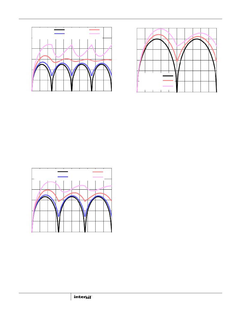
�FIGURE� 23.� NORMALIZED� INPUT-CAPACITOR� RMS� CURRENT� vs�
�DUTY� CYCLE� FOR� 4-PHASE� CONVERTER�
�For� a� four-phase� design,� use� Figure� 23� to� determine� the�
�input-capacitor� RMS� current� requirement� set� by� the� duty� cycle,�
�maximum� sustained� output� current� (I� O� ),� and� the� ratio� of� the�
�peak-to-peak� inductor� current� (I� L(P-P)� )� to� I� O� .� Select� a� bulk�
�capacitor� with� a� ripple� current� rating� which� will� minimize� the�
�total� number� of� input� capacitors� required� to� support� the� RMS�
�current� calculated.�
�The� voltage� rating� of� the� capacitors� should� also� be� at� least� 1.25x�
�greater� than� the� maximum� input� voltage.� Figures� 24� and� 25� provide�
�the� same� input� RMS� current� information� for� three-phase� and�
�2-phase� designs� respectively.� Use� the� same� approach� for� selecting�
�the� bulk� capacitor� type� and� number.�
�0.3�
�I� L(P-P)� =� 0� I� L(P-P)� =� 0.5� I� O�
�I� L(P-P)� =� 0.25� I� O� I� L(P-P)� =� 0.75� I� O�
�0.2�
�0.1�
�DUTY� CYCLE� (V� IN/� V� O� )�
�FIGURE� 25.� NORMALIZED� INPUT-CAPACITOR� RMS�
�CURRENT� FOR� 2-PHASE� CONVERTER�
�Layout� Considerations�
�MOSFETs� switch� very� fast� and� efficiently.� The� speed� with� which�
�the� current� transitions� from� one� device� to� another� causes� voltage�
�spikes� across� the� interconnecting� impedances� and� parasitic�
�circuit� elements.� These� voltage� spikes� can� degrade� efficiency,�
�radiate� noise� into� the� circuit� and� lead� to� device� overvoltage�
�stress.� Careful� component� selection,� layout,� and� placement�
�minimizes� these� voltage� spikes.� Consider,� as� an� example,� the�
�turnoff� transition� of� the� upper� PWM� MOSFET.� Prior� to� turnoff,� the�
�upper� MOSFET� was� carrying� channel� current.� During� the� turnoff,�
�current� stops� flowing� in� the� upper� MOSFET� and� is� picked� up� by�
�the� lower� MOSFET.� Any� inductance� in� the� switched� current� path�
�generates� a� large� voltage� spike� during� the� switching� interval.�
�Careful� component� selection,� tight� layout� of� the� critical�
�components,� and� short,� wide� circuit� traces� minimize� the�
�magnitude� of� voltage� spikes.�
�There� are� two� sets� of� critical� components� in� a� DC/DC� converter�
�using� a� ISL6328� controller.� The� power� components� are� the� most�
�critical� because� they� switch� large� amounts� of� energy.� Next� are�
�small� signal� components� that� connect� to� sensitive� nodes� or�
�supply� critical� bypassing� current� and� signal� coupling.�
�The� power� components� should� be� placed� first,� which� include� the�
�MOSFETs,� input� and� output� capacitors,� and� the� inductors.� It� is�
�important� to� have� a� symmetrical� layout� for� each� power� train,�
�preferably� with� the� controller� located� equidistant� from� each.�
�Symmetrical� layout� allows� heat� to� be� dissipated� equally� across� all�
�0�
�0� 0.2� 0.4� 0.6� 0.8�
�DUTY� CYCLE� (V� IN/� V� O� )�
�FIGURE� 24.� NORMALIZED� INPUT-CAPACITOR� RMS� CURRENT�
�FOR� 3-PHASE� CONVERTER�
�1.0�
�power� trains.� Equidistant� placement� of� the� controller� to� the� CORE�
�and� NB� power� trains� it� controls� through� the� integrated� drivers�
�helps� keep� the� gate� drive� traces� equally� short,� resulting� in� equal�
�trace� impedances� and� similar� drive� capability� of� all� sets� of�
�MOSFETs.�
�Low� capacitance,� high-frequency� ceramic� capacitors� are� needed� in�
�addition� to� the� input� bulk� capacitors� to� suppress� leading� and�
�falling� edge� voltage� spikes.� The� spikes� result� from� the� high� current�
�slew� rate� produced� by� the� upper� MOSFET� turn� on� and� off.� Select�
�low� ESL� ceramic� capacitors� and� place� one� as� close� as� possible� to�
�each� upper� MOSFET� drain� to� minimize� board� parasitics� and�
�maximize� suppression.�
�29�
�When� placing� the� MOSFETs� try� to� keep� the� source� of� the� upper�
�FETs� and� the� drain� of� the� lower� FETs� as� close� as� thermally� possible.�
�Input� high-frequency� capacitors,� C� HF� ,� should� be� placed� close� to� the�
�drain� of� the� upper� FETs� and� the� source� of� the� lower� FETs.� Input�
�bulk� capacitors,� CBULK,� case� size� typically� limits� following� the�
�same� rule� as� the� high-frequency� input� capacitors.� Place� the� input�
�FN7621.1�
�June� 7,� 2011�
�相关PDF资料 |
PDF描述 |
|---|---|
| ISL6329IRZ-T | IC CTRLR PWM SYNC BUCK DL 60QFN |
| ISL6333IRZ | IC CTRLR PWM 3PHASE BUCK 48-QFN |
| ISL6334AIRZR5368 | IC CTRLR PWM 4PHASE BUCK 40QFN |
| ISL6334BIRZ-T | IC CTRLR PWM SYNC BUCK 40-QFN |
| ISL6334CRZ | IC CTRLR PWM 4PHASE BUCK 40-QFN |
相关代理商/技术参数 |
参数描述 |
|---|---|
| ISL6328IRZ-T | 功能描述:IC CTRLR PWM SYNC BUCK DL 48QFN RoHS:是 类别:集成电路 (IC) >> PMIC - 稳压器 - 专用型 系列:- 标准包装:2,000 系列:- 应用:控制器,DSP 输入电压:4.5 V ~ 25 V 输出数:2 输出电压:最低可调至 1.2V 工作温度:-40°C ~ 85°C 安装类型:表面贴装 封装/外壳:30-TFSOP(0.173",4.40mm 宽) 供应商设备封装:30-TSSOP 包装:带卷 (TR) |
| ISL6329CRZ | 功能描述:电压模式 PWM 控制器 6+1 PHS DL PWM CONTRLR FOR CORE RoHS:否 制造商:Texas Instruments 输出端数量:1 拓扑结构:Buck 输出电压:34 V 输出电流: 开关频率: 工作电源电压:4.5 V to 5.5 V 电源电流:600 uA 最大工作温度:+ 125 C 最小工作温度:- 40 C 封装 / 箱体:WSON-8 封装:Reel |
| ISL6329CRZ-T | 功能描述:电压模式 PWM 控制器 6+1 PHS DL PWM CONTRLR FOR CORE RoHS:否 制造商:Texas Instruments 输出端数量:1 拓扑结构:Buck 输出电压:34 V 输出电流: 开关频率: 工作电源电压:4.5 V to 5.5 V 电源电流:600 uA 最大工作温度:+ 125 C 最小工作温度:- 40 C 封装 / 箱体:WSON-8 封装:Reel |
| ISL6329EVAL1Z | 制造商:Intersil Corporation 功能描述:ISL6329 EVALUATION BOARD - 60 LEAD - QFN - ROHS COMPLIANT - Bulk |
| ISL6329IRZ | 功能描述:电压模式 PWM 控制器 6+1 PHS DL PWM CONTRLR FOR CORE RoHS:否 制造商:Texas Instruments 输出端数量:1 拓扑结构:Buck 输出电压:34 V 输出电流: 开关频率: 工作电源电压:4.5 V to 5.5 V 电源电流:600 uA 最大工作温度:+ 125 C 最小工作温度:- 40 C 封装 / 箱体:WSON-8 封装:Reel |
发布紧急采购,3分钟左右您将得到回复。